- 您現(xiàn)在的位置:買賣IC網(wǎng) > PDF目錄68773 > 11274-001-XTP PLL FREQUENCY SYNTHESIZER, 28 MHz, PDSO16 PDF資料下載
參數(shù)資料
| 型號: | 11274-001-XTP |
| 元件分類: | PLL合成/DDS/VCOs |
| 英文描述: | PLL FREQUENCY SYNTHESIZER, 28 MHz, PDSO16 |
| 封裝: | 0.150 INCH, SOIC-16 |
| 文件頁數(shù): | 15/40頁 |
| 文件大小: | 746K |
| 代理商: | 11274-001-XTP |
第1頁第2頁第3頁第4頁第5頁第6頁第7頁第8頁第9頁第10頁第11頁第12頁第13頁第14頁當前第15頁第16頁第17頁第18頁第19頁第20頁第21頁第22頁第23頁第24頁第25頁第26頁第27頁第28頁第29頁第30頁第31頁第32頁第33頁第34頁第35頁第36頁第37頁第38頁第39頁第40頁
22
AMI Semiconductor - Rev. 2.0, Jun. 05
www.amis.com
FS6131-01/FS6131-01g Programmable Line Lock Clock Generator IC
Data Sheet
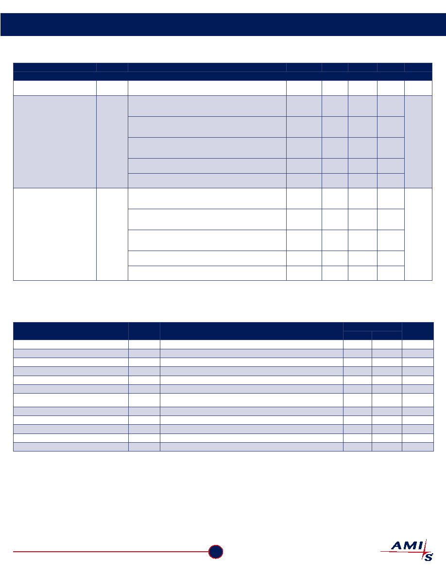
Table 15: AC Timing Specifications (Continued)
Parameter
Symbol
Conditions/Description
Clock (MHz)
Min.
Typ.
Max.
Units
Clock Output (CLKP, CLKN)
Duty cycle*
Ratio of pulse width (as measured from rising edge to next falling
edge at 2.5V) to one clock period
100
47
54
%
Jitter, long term (
sy(t))
tj(LT)
Rising edges 50ms apart at 2.5V, relative to an ideal clock, CL=15pF,
fREF=8kHz, NR=1, NF=193, NPx=64, CLF=0.054
mF, RLF=15.7kW,
CLP=1800pF, OSCTYPE=0, MLCP=3, XLROM=7
1.544
270
ps
Rising edges 50ms apart at 2.5V, relative to an ideal clock, CL=15pF,
fREF=15kHz, NR=1, NF=800, NPx=10, CLF=0.0246
mF, RLF=15.7kW,
CLP=820pF, OSCTYPE=0, MLCP=3, XLROM=7
12.00
160
On rising edges 5ms apart at 2.5V relative to an ideal clock,
CL=15pF, fREF=31.5kHz, NR=1, N=799, NPx=4, CLF=0.015
mF,
RLF=15.7k
W, CLP=470pF, OSCTYPE=0, MLCP=3, XLROM=7
25.175
100
On rising edges 500
ms apart at 2.5V relative to an ideal clock,
CL=15pF, CMOS mode, fXIN=27MHz, NF=200, NR=27, NPx=2
100
30
On rising edges 500
ms apart at 2.5V relative to an ideal clock,
CL=15pF, PECL mode, fXIN=27MHz, NF=200, NR=27, NPx=1
200
30
Jitter, period (peak-peak)*
tj(
DP)
From rising edge to next rising edge at 2.5V, CL=15pF, fREF=8kHz,
NR=1, NF=193, NPx=64, CLF=0.054
mF, RLF=15.7kW, CLP=1800pF,
OSCTYPE=0, MLCP=3, XLROM=7
1.544
140
ps
From rising edge to next rising edge at 2.5V, CL=15pF, fREF=15kHz,
NR=1, NF=800, NPx=10, CLF=0.0246
mF, RLF=15.7kW, CLP=820pF,
OSCTYPE=0, MLCP=3, XLROM=7
12.00
130
From rising edge to next rising edge at 2.5V, CL=15pF, fREF=31.5kHz,
NR=1, NF=799, NPx=4, CLF=0.015
mF, RLF=15.7kW, CLP=470pF,
OSCTYPE=0, MLCP=3, XLROM=7
25.175
105
From rising edge to next rising edge at 2.5V, CL=15pF, CMOS mode,
fXIN=27MHz, NF=200, NR=27, NPx=2
100
340
From rising edge to next rising edge at 2.5V, CL=15pF, PECL mode,
fXIN=27MHz, NF=200, NR=27, NPx=1
200
270
Unless otherwise stated, VDD = 5.0V ± 10%, no load on any output and ambient temperature range TA = 0°C to 70°C. Parameters denoted with an asterisk ( * ) represent nominal
characterization data and are not production tested to any specific limits. Min. and Max. characterization data are ± 3
s from typical.
Table 16: Serial Interface Timing Specifications
Parameter
Symbol
Conditions/Description
Standard Mode
Units
Min.
Max.
Clock frequency
fSCL
SCL
0
400
kHz
Bus free time between STOP and START
tBUF
4.7
ms
Setup time, START (repeated)
tsu:STA
4.7
ms
Hold time, START
thd:STA
4.0
ms
Setup time, data input
tsu:DAT
SDA
250
ns
Hold time, data input
thd:DAT
SDA
0
ms
Output data valid from clock
tAA
Minimum delay to bridge undefined region of the falling edge of SCL to avoid
unintended START or STOP
3.5
ms
Rise time, data and clock
tR
SDA, SCL
1000
ns
Fall time, data and clock
tF
SDA, SCL
300
ns
High time, clock
tHI
SCL
4.0
ms
Low time, clock
tLO
SCL
4.7
ms
Setup time, STOP
tsu:STO
4.0
ms
Unless otherwise stated, VDD = 5.0V ± 10%, no load on any output and ambient temperature range TA = 0°C to 70°C. Parameters denoted with an asterisk ( * ) represent nominal
characterization data and are not production tested to any specific limits. Min. and Max. characterization data are ± 3
s from typical.
相關(guān)PDF資料 |
PDF描述 |
|---|---|
| 11610 | BEZEL IEC CONN |
| 116450-01 | 130MM BLOWER 24 VDC |
| 116521-02 | 130MM BLOWER 24 VDC |
| 116629-03 | 145 MM 120V 250W TF BLOWER |
| 116630-06 | 145 MM 120V 250W TF BLOWER |
相關(guān)代理商/技術(shù)參數(shù) |
參數(shù)描述 |
|---|---|
| 1127-40-0516 | 制造商:Concord Electronics Inc 功能描述: |
| 1127-40-0519 | 制造商:Concord Electronics Inc 功能描述: |
| 11274-011 | 制造商:未知廠家 制造商全稱:未知廠家 功能描述:Programmable Line Lock Clock Generator IC |
| 112740-12 | 功能描述:RF 連接器 BNC END LAUNCH JACK 16MM HEX .062 PCB RoHS:否 制造商:Bomar Interconnect 產(chǎn)品:Connectors 射頻系列:BNC 型式:Jack (Female) 極性: 觸點電鍍:Gold 阻抗: 端接類型:Solder 主體類型:Straight Bulkhead 電纜類型: |
| 112740-13 | 功能描述:RF 連接器 BNC END LAUNCH JACK 14MM HEX .062 PCB RoHS:否 制造商:Bomar Interconnect 產(chǎn)品:Connectors 射頻系列:BNC 型式:Jack (Female) 極性: 觸點電鍍:Gold 阻抗: 端接類型:Solder 主體類型:Straight Bulkhead 電纜類型: |
發(fā)布緊急采購,3分鐘左右您將得到回復(fù)。