- 您現(xiàn)在的位置:買賣IC網(wǎng) > PDF目錄353028 > CY7C1069AV33-8BAC (CYPRESS SEMICONDUCTOR CORP) 2M x 8 Static RAM PDF資料下載
參數(shù)資料
| 型號(hào): | CY7C1069AV33-8BAC |
| 廠商: | CYPRESS SEMICONDUCTOR CORP |
| 元件分類: | DRAM |
| 英文描述: | 2M x 8 Static RAM |
| 中文描述: | 2M X 8 STANDARD SRAM, 8 ns, PBGA48 |
| 封裝: | 8 X 20 MM, 1.20 MM HEIGHT, FBGA-48 |
| 文件頁(yè)數(shù): | 4/9頁(yè) |
| 文件大小: | 249K |
| 代理商: | CY7C1069AV33-8BAC |
CY7C1069AV33
Document #: 38-05255 Rev. *D
Page 4 of 9
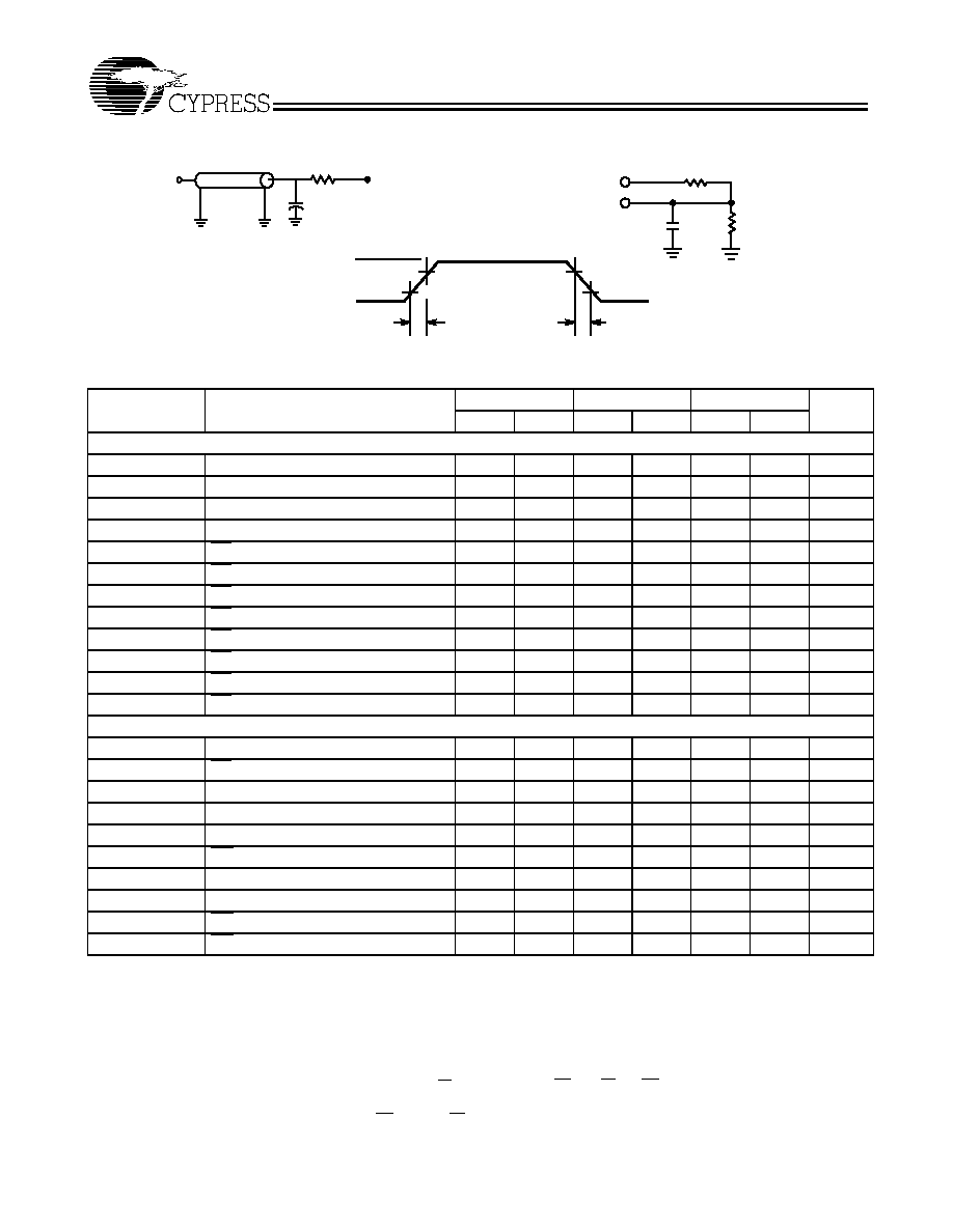
AC Test Loads and Waveforms[3]
AC Switching Characteristics Over the Operating Range [4]
Parameter
Description
–8
–10
–12
Unit
Min.
Max.
Min.
Max.
Min.
Max.
Read Cycle
tpower
VCC(typical) to the First Access
[5]
111
ms
tRC
Read Cycle Time
8
10
12
ns
tAA
Address to Data Valid
10
12
ns
tOHA
Data Hold from Address Change
3
ns
tACE
CE1 LOW/CE2 HIGH to Data Valid
8
10
12
ns
tDOE
OE LOW to Data Valid
5
6
ns
tLZOE
OE LOW to Low-Z[6]
111
ns
tHZOE
OE HIGH to High-Z[6]
55
6
ns
tLZCE
CE1 LOW/CE2 HIGH to Low-Z
[6]
333
ns
tHZCE
CE1 HIGH/CE2 LOW to High-Z
[6]
55
6
ns
tPU
CE1 LOW/CE2 HIGH to Power-up
[7]
000
ns
tPD
CE1 HIGH/CE2 LOW to Power-down
[7]
810
12
ns
Write Cycle[8, 9]
tWC
Write Cycle Time
8
10
12
ns
tSCE
CE1 LOW/CE2 HIGH to Write End
6
7
8
ns
tAW
Address Set-up to Write End
6
7
8
ns
tHA
Address Hold from Write End
0
ns
tSA
Address Set-up to Write Start
0
ns
tPWE
WE Pulse Width
6
7
8
ns
tSD
Data Set-up to Write End
5
5.5
6
ns
tHD
Data Hold from Write End
0
ns
tLZWE
WE HIGH to Low-Z[6]
333
ns
tHZWE
WE LOW to High-Z[6]
55
6
ns
Notes:
3.
Valid SRAM operation does not occur until the power supplies have reached the minimum operating VDD (3.0V). As soon as 1ms (Tpower) after reaching the
minimum operating VDD , normal SRAM operation can begin including reduction in VDD to the data retention (VCCDR, 2.0V) voltage.
4.
Test conditions assume signal transition time of 3 ns or less, timing reference levels of 1.5V, input pulse levels of 0 to 3.0V, and output loading of the specified
IOL/IOH and transmission line loads. Test conditions for the Read cycle use output loading shown in part a) of the AC test loads, unless specified otherwise.
5.
This part has a voltage regulator which steps down the voltage from 3V to 2V internally. tpower time has to be provided initially before a Read/Write operation
is started.
6.
tHZOE, tHZSCE, tHZWE and tLZOE, tLZCE, and tLZWE are specified with a load capacitance of 5 pF as in (b) of AC Test Loads. Transition is measured ±200 mV
from steady-state voltage.
7.
These parameters are guaranteed by design and are not tested.
8.
The internal Write time of the memory is defined by the overlap of CE1 LOW / CE2 HIGH, and WE LOW. CE1 and WE must be LOW along with CE2 HIGH to initiate
a Write, and the transition of any of these signals can terminate the Write. The input data set-up and hold timing should be referenced to the leading edge of
the signal that terminates the Write.
9.
The minimum Write cycle time for Write Cycle No. 3 (WE controlled, OE LOW) is the sum of tHZWE and tSD.
90%
10%
3.3V
GND
90%
10%
All input pulses
3.3V
OUTPUT
5 pF*
*Including
jig and
scope
(a)
(b)
R1 317
R2
351
Rise time > 1V/ns
Fall time:
> 1V/ns
(c)
OUTPUT
50
Z0= 50
VTH = 1.5V
30 pF*
*Capacitive Load consists of all
components of the test environment
相關(guān)PDF資料 |
PDF描述 |
|---|---|
| CY7C1069AV33-8BAI | 2M x 8 Static RAM |
| CY7C1069AV33-8ZC | 2M x 8 Static RAM |
| CY7C1069AV33-8ZI | 2M x 8 Static RAM |
| CY37128VP160-200BBXC | 5V, 3.3V, ISRTM High-Performance CPLDs |
| CY37256VP160-200BBXC | 5V, 3.3V, ISRTM High-Performance CPLDs |
相關(guān)代理商/技術(shù)參數(shù) |
參數(shù)描述 |
|---|---|
| CY7C1069AV33-8ZXC | 功能描述:IC SRAM 16MBIT 8NS 54TSOP RoHS:是 類別:集成電路 (IC) >> 存儲(chǔ)器 系列:- 標(biāo)準(zhǔn)包裝:1,000 系列:- 格式 - 存儲(chǔ)器:RAM 存儲(chǔ)器類型:移動(dòng) SDRAM 存儲(chǔ)容量:256M(8Mx32) 速度:133MHz 接口:并聯(lián) 電源電壓:1.7 V ~ 1.95 V 工作溫度:-40°C ~ 85°C 封裝/外殼:90-VFBGA 供應(yīng)商設(shè)備封裝:90-VFBGA(8x13) 包裝:帶卷 (TR) 其它名稱:557-1327-2 |
| CY7C1069AV33-8ZXCT | 制造商:Cypress Semiconductor 功能描述:SRAM ASYNC SGL 3.3V 16MBIT 2MX8 8NS 54TSOP-II - Tape and Reel |
| CY7C1069BV33-10ZXC | 制造商:Cypress Semiconductor 功能描述: |
| CY7C1069BV33-10ZXI | 制造商:Cypress Semiconductor 功能描述: |
| CY7C1069BV33-12ZC | 制造商:Rochester Electronics LLC 功能描述: 制造商:Cypress Semiconductor 功能描述: |
發(fā)布緊急采購(gòu),3分鐘左右您將得到回復(fù)。