- 您現(xiàn)在的位置:買賣IC網(wǎng) > PDF目錄379064 > CY7C1355C-100BZXI (CYPRESS SEMICONDUCTOR CORP) 9-Mbit (256K x 36/512K x 18) Flow-Through SRAM with NoBL⑩ Architecture PDF資料下載
參數(shù)資料
| 型號: | CY7C1355C-100BZXI |
| 廠商: | CYPRESS SEMICONDUCTOR CORP |
| 元件分類: | DRAM |
| 英文描述: | 9-Mbit (256K x 36/512K x 18) Flow-Through SRAM with NoBL⑩ Architecture |
| 中文描述: | 256K X 36 ZBT SRAM, 7.5 ns, PBGA165 |
| 封裝: | 13 X 15 MM, 1.40 MM HEIGHT, LEAD FREE, MO-216, FBGA-165 |
| 文件頁數(shù): | 14/28頁 |
| 文件大?。?/td> | 456K |
| 代理商: | CY7C1355C-100BZXI |
第1頁第2頁第3頁第4頁第5頁第6頁第7頁第8頁第9頁第10頁第11頁第12頁第13頁當(dāng)前第14頁第15頁第16頁第17頁第18頁第19頁第20頁第21頁第22頁第23頁第24頁第25頁第26頁第27頁第28頁
CY7C1355C
CY7C1357C
Document #: 38-05539 Rev. *E
Page 14 of 28
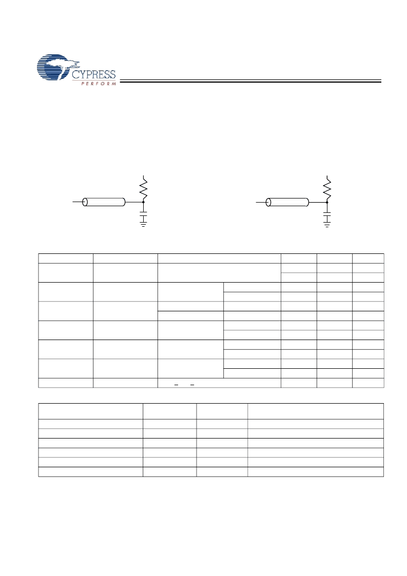
3.3V TAP AC Test Conditions
Input pulse levels................................................ V
SS
to 3.3V
Input rise and fall times................................................... 1 ns
Input timing reference levels...........................................1.5V
Output reference levels...................................................1.5V
Test load termination supply voltage...............................1.5V
3.3V TAP AC Output Load Equivalent
2.5V TAP AC Test Conditions
Input pulse levels.................................................V
SS
to 2.5V
Input rise and fall time .....................................................1 ns
Input timing reference levels.........................................1.25V
Output reference levels ................................................1.25V
Test load termination supply voltage ............................1.25V
2.5V TAP AC Output Load Equivalent
TDO
1.5V
20pF
Z = 50
50
TDO
1.25V
20pF
Z = 50
50
TAP DC Electrical Characteristics
And Operating Conditions
(0°C < T
A
< +70°C; V
DD
= 3.3V ± 0.165V unless
otherwise noted)
[12]
Parameter
V
OH1
Description
Output HIGH Voltage
Conditions
Min.
2.4
2.0
2.9
2.1
Max.
Unit
V
V
V
V
V
V
V
V
V
V
V
V
μA
I
OH
= –4.0 mA, V
DDQ
= 3.3V
I
OH
= –1.0 mA, V
DDQ
= 2.5V
V
OH2
Output HIGH Voltage
I
OH
= –100 μA
V
DDQ
= 3.3V
V
DDQ
= 2.5V
V
DDQ
= 3.3V
V
DDQ
= 2.5V
V
DDQ
= 3.3V
V
DDQ
= 2.5V
V
DDQ
= 3.3V
V
DDQ
= 2.5V
V
DDQ
= 3.3V
V
DDQ
= 2.5V
V
OL1
Output LOW Voltage
I
OL
= 8.0 mA
I
OL
= 8.0 mA
I
OL
= 100 μA
0.4
0.4
0.2
0.2
V
OL2
Output LOW Voltage
V
IH
Input HIGH Voltage
2.0
1.7
–0.5
–0.3
–5
V
DD
+ 0.3
V
DD
+ 0.3
0.7
0.7
5
V
IL
Input LOW Voltage
I
X
Input Load Current
GND < V
IN
< V
DDQ
Identification Register Definitions
Instruction Field
CY7C1355C
(256Kx36)
010
01010
001001
100110
00000110100
1
CY7C1357C
(512Kx18)
010
01010
001001
010110
00000110100
1
Description
Revision Number (31:29)
Device Depth (28:24)
Device Width (23:18)
Cypress Device ID (17:12)
Cypress JEDEC ID Code (11:1)
ID Register Presence Indicator (0)
Describes the version number
Reserved for Internal Use
Defines memory type and architecture
Defines width and density
Allows unique identification of SRAM vendor
Indicates the presence of an ID register
Note:
12.All voltages referenced to V
SS
(GND).
[+] Feedback
相關(guān)PDF資料 |
PDF描述 |
|---|---|
| CY7C1355C-133AXC | 9-Mbit (256K x 36/512K x 18) Flow-Through SRAM with NoBL⑩ Architecture |
| CY7C1355C-133AXI | 9-Mbit (256K x 36/512K x 18) Flow-Through SRAM with NoBL⑩ Architecture |
| CY7C1355C-133BGXC | 9-Mbit (256K x 36/512K x 18) Flow-Through SRAM with NoBL⑩ Architecture |
| CY7C1355C-133BGXI | 9-Mbit (256K x 36/512K x 18) Flow-Through SRAM with NoBL⑩ Architecture |
| CY7C1355C-133BZXC | 9-Mbit (256K x 36/512K x 18) Flow-Through SRAM with NoBL⑩ Architecture |
相關(guān)代理商/技術(shù)參數(shù) |
參數(shù)描述 |
|---|---|
| CY7C1355C-133AXC | 功能描述:靜態(tài)隨機(jī)存取存儲(chǔ)器 256Kx36 3.3V NoBL Sync FT 靜態(tài)隨機(jī)存取存儲(chǔ)器 COM RoHS:否 制造商:Cypress Semiconductor 存儲(chǔ)容量:16 Mbit 組織:1 M x 16 訪問時(shí)間:55 ns 電源電壓-最大:3.6 V 電源電壓-最小:2.2 V 最大工作電流:22 uA 最大工作溫度:+ 85 C 最小工作溫度:- 40 C 安裝風(fēng)格:SMD/SMT 封裝 / 箱體:TSOP-48 封裝:Tray |
| CY7C1355C-133AXCKJ | 制造商:Cypress Semiconductor 功能描述: |
| CY7C1355C-133AXCT | 功能描述:靜態(tài)隨機(jī)存取存儲(chǔ)器 256Kx36 3.3V NoBL Sync FT 靜態(tài)隨機(jī)存取存儲(chǔ)器 COM RoHS:否 制造商:Cypress Semiconductor 存儲(chǔ)容量:16 Mbit 組織:1 M x 16 訪問時(shí)間:55 ns 電源電壓-最大:3.6 V 電源電壓-最小:2.2 V 最大工作電流:22 uA 最大工作溫度:+ 85 C 最小工作溫度:- 40 C 安裝風(fēng)格:SMD/SMT 封裝 / 箱體:TSOP-48 封裝:Tray |
| CY7C1355C-133AXI | 制造商:Rochester Electronics LLC 功能描述: 制造商:Cypress Semiconductor 功能描述: |
| CY7C1355C-133AXIT | 制造商:Rochester Electronics LLC 功能描述: 制造商:Cypress Semiconductor 功能描述: |
發(fā)布緊急采購,3分鐘左右您將得到回復(fù)。