- 您現(xiàn)在的位置:買賣IC網(wǎng) > PDF目錄379068 > CY7C1370D-250AXC (CYPRESS SEMICONDUCTOR CORP) 18-Mbit (512K X 36/1M X 18) Pipelined SRAM with NoBL Architecture PDF資料下載
參數(shù)資料
| 型號(hào): | CY7C1370D-250AXC |
| 廠商: | CYPRESS SEMICONDUCTOR CORP |
| 元件分類: | DRAM |
| 英文描述: | 18-Mbit (512K X 36/1M X 18) Pipelined SRAM with NoBL Architecture |
| 中文描述: | 512K X 36 ZBT SRAM, 2.6 ns, PQFP100 |
| 封裝: | 14 X 20 MM, 1.40 MM HEIGHT, LEAD FREE, PLASTIC, MS-026, TQFP-100 |
| 文件頁數(shù): | 10/30頁 |
| 文件大?。?/td> | 344K |
| 代理商: | CY7C1370D-250AXC |
第1頁第2頁第3頁第4頁第5頁第6頁第7頁第8頁第9頁當(dāng)前第10頁第11頁第12頁第13頁第14頁第15頁第16頁第17頁第18頁第19頁第20頁第21頁第22頁第23頁第24頁第25頁第26頁第27頁第28頁第29頁第30頁
PRELIMINARY
CY7C1370D
CY7C1372D
Document #: 38-05555 Rev. *A
Page 10 of 30
IEEE 1149.1 Serial Boundary Scan (JTAG)
The CY7C1370D/CY7C1372D incorporates a serial boundary
scan test access port (TAP). This part is fully compliant with
1149.1. The TAP operates using JEDEC-standard 3.3V or
2.5V I/O logic levels.
The CY7C1370D/CY7C1372D contains a TAP controller,
instruction register, boundary scan register, bypass register,
and ID register.
Disabling the JTAG Feature
It is possible to operate the SRAM without using the JTAG
feature. To disable the TAP controller, TCK must be tied
LOW(V
SS
) to prevent clocking of the device. TDI and TMS are
internally pulled up and may be unconnected. They may alter-
nately be connected to V
DD
through a pull-up resistor. TDO
should be left unconnected. Upon power-up, the device will
come up in a reset state which will not interfere with the
operation of the device.
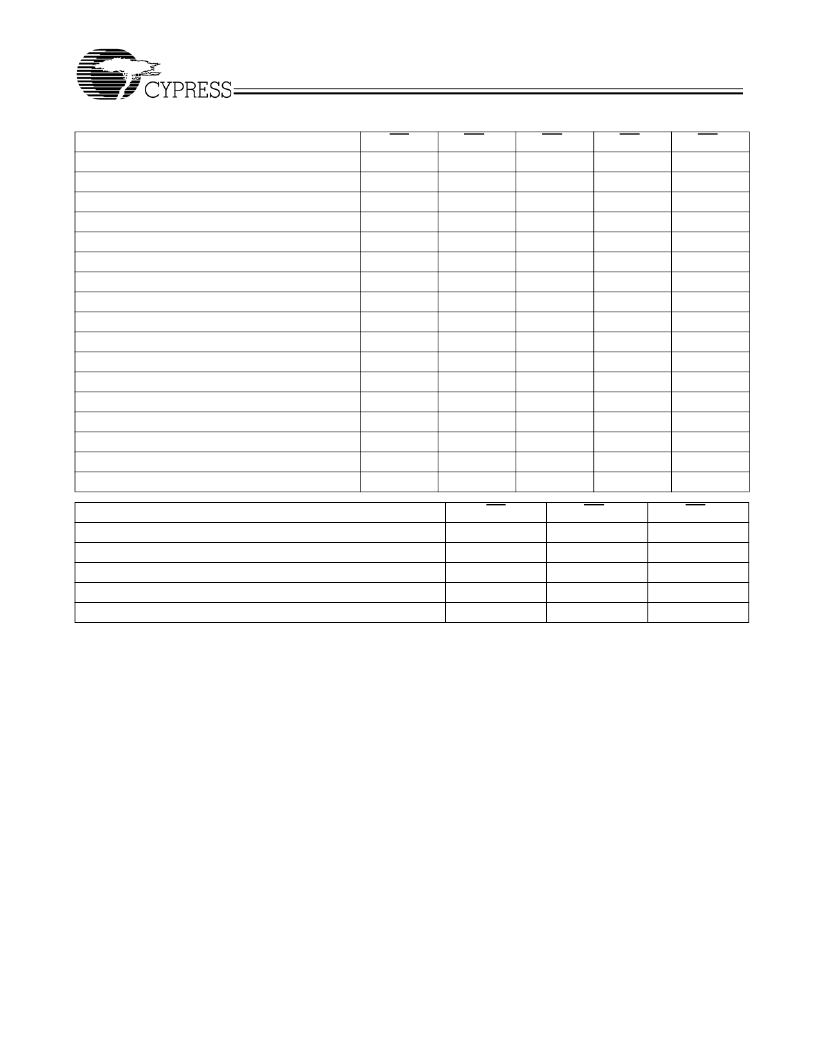
Partial Write Cycle Description
[1, 2, 3, 8]
Function (CY7C1370D)
WE
H
L
BW
d
X
H
BW
c
X
H
BW
b
X
H
BW
a
X
H
Read
Write – No bytes written
Write Byte a – (DQ
a
and
DQP
a
)
Write Byte b – (DQ
b
and
DQP
b
)
Write Bytes b, a
Write Byte c – (DQ
c
and
DQP
c
)
Write Bytes c, a
Write Bytes c, b
Write Bytes c, b, a
Write Byte d – (DQ
d
and
DQP
d
)
Write Bytes d, a
Write Bytes d, b
Write Bytes d, b, a
Write Bytes d, c
Write Bytes d, c, a
Write Bytes d, c, b
Write All Bytes
L
L
L
L
L
L
L
L
L
L
L
L
L
L
L
H
H
H
H
H
H
H
L
L
L
L
L
L
L
L
H
H
H
L
L
L
L
H
H
H
H
L
L
L
L
H
L
L
H
H
L
L
H
H
L
L
H
H
L
L
L
H
L
H
L
H
L
H
L
H
L
H
L
H
L
Function (CY7C1372D)
WE
H
L
L
L
L
BW
b
x
H
H
L
L
BW
a
x
H
L
H
L
Read
Write – No Bytes Written
Write Byte a – (DQ
a
and
DQP
a
)
Write Byte b – (DQ
b
and
DQP
b
)
Write Both Bytes
相關(guān)PDF資料 |
PDF描述 |
|---|---|
| CY7C1381DV25-133BZI | 18-Mbit (512K x 36/1M x 18) Flow-Through SRAM |
| CY7C1383FV25-100BGC | 18-Mbit (512K x 36/1M x 18) Flow-Through SRAM |
| CY7C1383FV25-100BGI | 18-Mbit (512K x 36/1M x 18) Flow-Through SRAM |
| CY7C1383FV25-100BGXC | 18-Mbit (512K x 36/1M x 18) Flow-Through SRAM |
| CY7C1383FV25-100BGXI | 18-Mbit (512K x 36/1M x 18) Flow-Through SRAM |
相關(guān)代理商/技術(shù)參數(shù) |
參數(shù)描述 |
|---|---|
| CY7C1370D-250AXCT | 功能描述:靜態(tài)隨機(jī)存取存儲(chǔ)器 512Kx36 3.3V NoBL Sync PL 靜態(tài)隨機(jī)存取存儲(chǔ)器 COM RoHS:否 制造商:Cypress Semiconductor 存儲(chǔ)容量:16 Mbit 組織:1 M x 16 訪問時(shí)間:55 ns 電源電壓-最大:3.6 V 電源電壓-最小:2.2 V 最大工作電流:22 uA 最大工作溫度:+ 85 C 最小工作溫度:- 40 C 安裝風(fēng)格:SMD/SMT 封裝 / 箱體:TSOP-48 封裝:Tray |
| CY7C1370D-250AXI | 功能描述:靜態(tài)隨機(jī)存取存儲(chǔ)器 18Mbit Pipeline 靜態(tài)隨機(jī)存取存儲(chǔ)器 w/ NoBL RoHS:否 制造商:Cypress Semiconductor 存儲(chǔ)容量:16 Mbit 組織:1 M x 16 訪問時(shí)間:55 ns 電源電壓-最大:3.6 V 電源電壓-最小:2.2 V 最大工作電流:22 uA 最大工作溫度:+ 85 C 最小工作溫度:- 40 C 安裝風(fēng)格:SMD/SMT 封裝 / 箱體:TSOP-48 封裝:Tray |
| CY7C1370D-250BZC | 制造商:Cypress Semiconductor 功能描述:SRAM SYNC QUAD 3.3V 18MBIT 512KX36 2.6NS 165FBGA - Bulk |
| CY7C1370DV25-167 | 制造商:Cypress Semiconductor 功能描述: |
| CY7C1370DV25-167AXC | 功能描述:靜態(tài)隨機(jī)存取存儲(chǔ)器 512Kx36 2.5V NoBL Sync PL 靜態(tài)隨機(jī)存取存儲(chǔ)器 COM RoHS:否 制造商:Cypress Semiconductor 存儲(chǔ)容量:16 Mbit 組織:1 M x 16 訪問時(shí)間:55 ns 電源電壓-最大:3.6 V 電源電壓-最小:2.2 V 最大工作電流:22 uA 最大工作溫度:+ 85 C 最小工作溫度:- 40 C 安裝風(fēng)格:SMD/SMT 封裝 / 箱體:TSOP-48 封裝:Tray |
發(fā)布緊急采購,3分鐘左右您將得到回復(fù)。