- 您現(xiàn)在的位置:買賣IC網(wǎng) > PDF目錄379080 > CY7C1483V33-100BZI (CYPRESS SEMICONDUCTOR CORP) 72-Mbit (2M x 36/4M x 18/1M x 72) Flow-Through SRAM PDF資料下載
參數(shù)資料
| 型號: | CY7C1483V33-100BZI |
| 廠商: | CYPRESS SEMICONDUCTOR CORP |
| 元件分類: | DRAM |
| 英文描述: | 72-Mbit (2M x 36/4M x 18/1M x 72) Flow-Through SRAM |
| 中文描述: | 4M X 18 CACHE SRAM, 8.5 ns, PBGA165 |
| 封裝: | 15 X 17 MM, 1.40 MM HEIGHT, FBGA-165 |
| 文件頁數(shù): | 10/30頁 |
| 文件大?。?/td> | 998K |
| 代理商: | CY7C1483V33-100BZI |
第1頁第2頁第3頁第4頁第5頁第6頁第7頁第8頁第9頁當前第10頁第11頁第12頁第13頁第14頁第15頁第16頁第17頁第18頁第19頁第20頁第21頁第22頁第23頁第24頁第25頁第26頁第27頁第28頁第29頁第30頁
CY7C1481V33
CY7C1483V33
CY7C1487V33
Document #: 38-05284 Rev. *H
Page 10 of 30
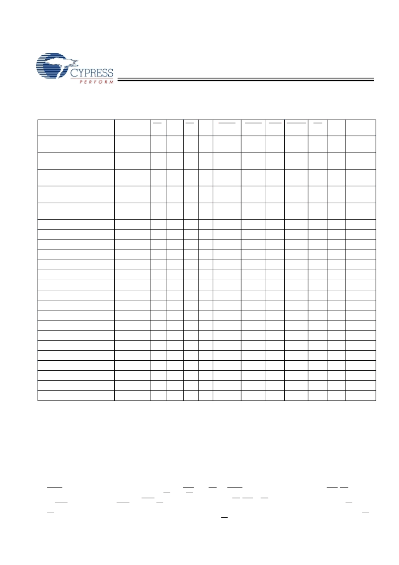
Truth Table
The truth table for CY7C1481V33, CY7C1483V33, and CY7C1487V33 follows.
[3, 4, 5, 6, 7]
Cycle Description
ADDRESS
Used
CE
1
CE
2
CE
3
ZZ
ADSP
ADSC
ADV WRITE
OE
CLK
DQ
Deselected Cycle,
Power Down
None
H
X
X
L
X
L
X
X
X
L-H
Tri-State
Deselected Cycle,
Power Down
None
L
L
X
L
L
X
X
X
X
L-H
Tri-State
Deselected Cycle,
Power Down
None
L
X
H
L
L
X
X
X
X
L-H
Tri-State
Deselected Cycle,
Power Down
None
L
L
X
L
H
L
X
X
X
L-H
Tri-State
Deselected Cycle,
Power Down
None
X
X
X
L
H
L
X
X
X
L-H
Tri-State
Sleep Mode, Power Down
None
X
X
X
H
X
X
X
X
X
X
Tri-State
Read Cycle, Begin Burst
External
L
H
L
L
L
X
X
X
L
L-H
Q
Read Cycle, Begin Burst
External
L
H
L
L
L
X
X
X
H
L-H
Tri-State
Write Cycle, Begin Burst
External
L
H
L
L
H
L
X
L
X
L-H
D
Read Cycle, Begin Burst
External
L
H
L
L
H
L
X
H
L
L-H
Q
Read Cycle, Begin Burst
External
L
H
L
L
H
L
X
H
H
L-H
Tri-State
Read Cycle, Continue Burst
Next
X
X
X
L
H
H
L
H
L
L-H
Q
Read Cycle, Continue Burst
Next
X
X
X
L
H
H
L
H
H
L-H
Tri-State
Read Cycle, Continue Burst
Next
H
X
X
L
X
H
L
H
L
L-H
Q
Read Cycle, Continue Burst
Next
H
X
X
L
X
H
L
H
H
L-H
Tri-State
Write Cycle, Continue Burst
Next
X
X
X
L
H
H
L
L
X
L-H
D
Write Cycle, Continue Burst
Next
H
X
X
L
X
H
L
L
X
L-H
D
Read Cycle, Suspend Burst
Current
X
X
X
L
H
H
H
H
L
L-H
Q
Read Cycle, Suspend Burst
Current
X
X
X
L
H
H
H
H
H
L-H
Tri-State
Read Cycle, Suspend Burst
Current
H
X
X
L
X
H
H
H
L
L-H
Q
Read Cycle, Suspend Burst
Current
H
X
X
L
X
H
H
H
H
L-H
Tri-State
Write Cycle, Suspend Burst
Current
X
X
X
L
H
H
H
L
X
L-H
D
Write Cycle, Suspend Burst
Current
H
X
X
L
X
H
H
L
X
L-H
D
Notes
3. X = Do Not Care, H = Logic HIGH, L = Logic LOW.
4. WRITE = L when any one or more Byte Write Enable signals and BWE = L or GW = L. WRITE = H when all Byte Write Enable signals, BWE, GW = H.
5. The DQ pins are controlled by the current cycle and the OE signal. OE is asynchronous and is not sampled with the clock.
6. The SRAM always initiates a read cycle when ADSP is asserted, regardless of the state of GW, BWE, or BW
. Writes may occur only on subsequent clocks after
the ADSP or with the assertion of ADSC. As a result, OE must be driven HIGH prior to the start of the write cycle to enable the outputs to tri-state. OE is a do not
care for the remainder of the write cycle.
7. OE is asynchronous and is not sampled with the clock rise. It is masked internally during write cycles. During a read cycle all data bits are tri-state when OE is
inactive or when the device is deselected, and all data bits behave as outputs when OE is active (LOW).
[+] Feedback
相關(guān)PDF資料 |
PDF描述 |
|---|---|
| CY7C1483V33-100BZXC | 72-Mbit (2M x 36/4M x 18/1M x 72) Flow-Through SRAM |
| CY7C1483V33-100BZXI | 72-Mbit (2M x 36/4M x 18/1M x 72) Flow-Through SRAM |
| CY7C1483V33-133AXC | 72-Mbit (2M x 36/4M x 18/1M x 72) Flow-Through SRAM |
| CY7C1483V33-133AXI | 72-Mbit (2M x 36/4M x 18/1M x 72) Flow-Through SRAM |
| CY7C1483V33-133BZI | 72-Mbit (2M x 36/4M x 18/1M x 72) Flow-Through SRAM |
相關(guān)代理商/技術(shù)參數(shù) |
參數(shù)描述 |
|---|---|
| CY7C148-45DC | 制造商:Cypress Semiconductor 功能描述:Static RAM, 1Kx4, 18 Pin, Ceramic, DIP |
| CY7C148-45PC | 制造商:Cypress Semiconductor 功能描述: |
| CY7C1484BV25-250AXI | 制造商:Cypress Semiconductor 功能描述:SYNC - Trays 制造商:Cypress Semiconductor 功能描述:IC SRAM 72MBIT 250MHZ 100TQFP 制造商:Cypress Semiconductor 功能描述:TRAY / Sync SRAMs |
| CY7C1484BV33-250BZI | 制造商:Cypress Semiconductor 功能描述: |
| CY7C1484BV33-250BZXC | 功能描述:靜態(tài)隨機存取存儲器 72MB (2Mx36) 3.3v 250MHz 靜態(tài)隨機存取存儲器 RoHS:否 制造商:Cypress Semiconductor 存儲容量:16 Mbit 組織:1 M x 16 訪問時間:55 ns 電源電壓-最大:3.6 V 電源電壓-最小:2.2 V 最大工作電流:22 uA 最大工作溫度:+ 85 C 最小工作溫度:- 40 C 安裝風格:SMD/SMT 封裝 / 箱體:TSOP-48 封裝:Tray |
發(fā)布緊急采購,3分鐘左右您將得到回復(fù)。