- 您現(xiàn)在的位置:買賣IC網(wǎng) > PDF目錄379081 > CY7C1510AV18-167BZC (CYPRESS SEMICONDUCTOR CORP) 72-Mbit QDR-II⑩ SRAM 2-Word Burst Architecture PDF資料下載
參數(shù)資料
| 型號: | CY7C1510AV18-167BZC |
| 廠商: | CYPRESS SEMICONDUCTOR CORP |
| 元件分類: | DRAM |
| 英文描述: | 72-Mbit QDR-II⑩ SRAM 2-Word Burst Architecture |
| 中文描述: | 8M X 8 QDR SRAM, 0.5 ns, PBGA165 |
| 封裝: | 15 X 17 MM, 1.40 MM HEIGHT, MO-216, FBGA-165 |
| 文件頁數(shù): | 21/26頁 |
| 文件大小: | 1074K |
| 代理商: | CY7C1510AV18-167BZC |
第1頁第2頁第3頁第4頁第5頁第6頁第7頁第8頁第9頁第10頁第11頁第12頁第13頁第14頁第15頁第16頁第17頁第18頁第19頁第20頁當(dāng)前第21頁第22頁第23頁第24頁第25頁第26頁
PRELIMINARY
CY7C1510AV18
CY7C1525AV18
CY7C1512AV18
CY7C1514AV18
Document #: 001-06984 Rev. *B
Page 21 of 26
Thermal Resistance
[21]
Parameter
Θ
JA
Description
Test Conditions
165 FBGA Package
16.2
Unit
°
C/W
Thermal Resistance
(Junction to Ambient)
Thermal Resistance
(Junction to Case)
Test conditions follow standard test
methods and procedures for
measuring thermal impedance, per
EIA/ JESD51.
Θ
JC
2.3
°
C/W
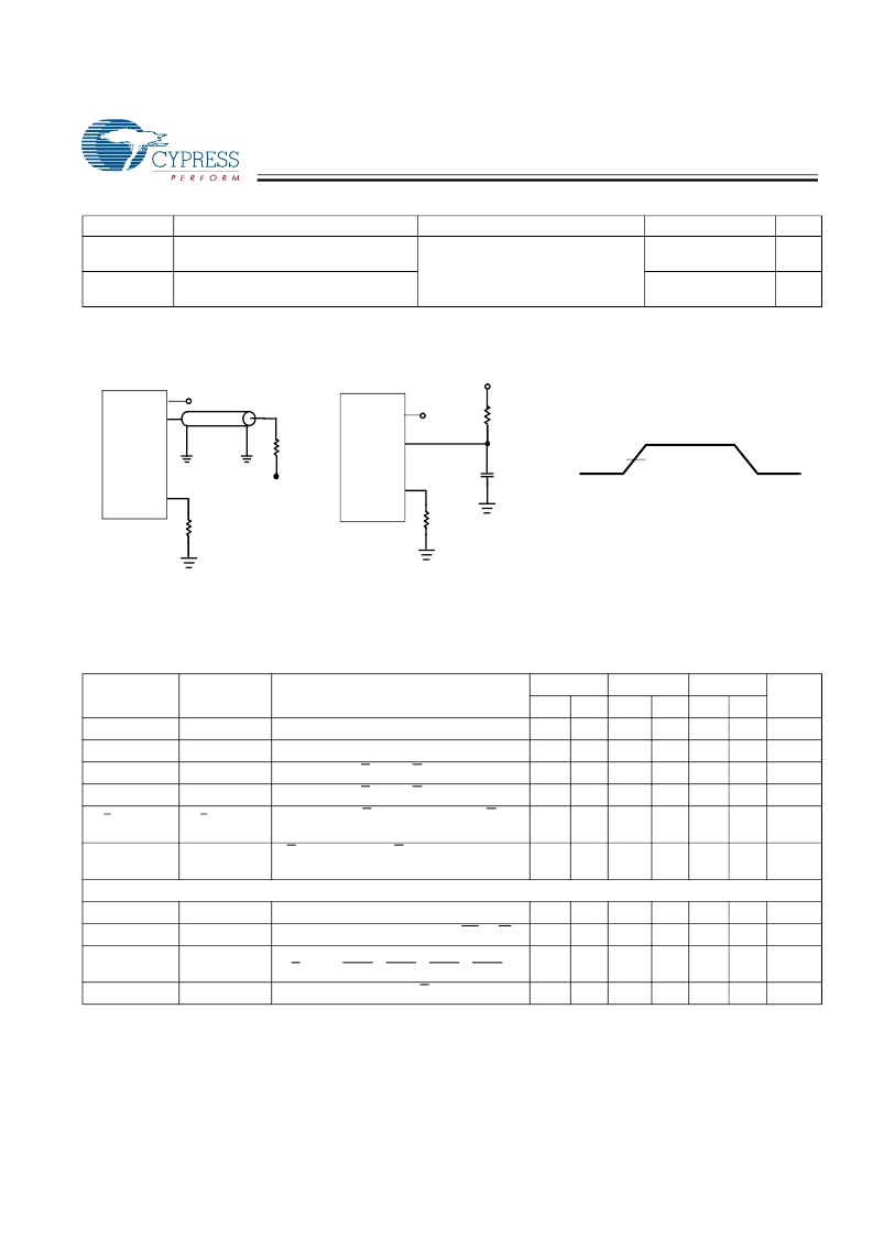
AC Test Loads and Waveforms
Switching Characteristics
Over the Operating Range
[22, 23]
Cypress
Parameter
t
POWER
t
CYC
t
KH
t
KL
t
KHKH
Consortium
Parameter
Description
250 MHz
Min.
1
4.0
1.6
1.6
1.8
200 MHz
Min.
1
5.0
2.0
2.0
2.2
167 MHz
Min.
1
6.0
2.4
2.4
2.7
Unit
ms
ns
ns
ns
ns
Max
Max
Max
V
DD
(Typical) to the first Access
[24]
K Clock and C Clock Cycle Time
Input Clock (K/K and C/C) HIGH
Input Clock (K/K and C/C) LOW
K Clock Rise to K Clock Rise and C to C Rise
(rising edge to rising edge)
K/K Clock Rise to C/C Clock Rise (rising
edge to rising edge)
t
KHKH
t
KHKL
t
KLKH
t
KHKH
6.3
–
–
–
7.9
–
–
–
8.4
–
–
–
t
KHCH
t
KHCH
0
1.8
0
2.2
0
2.7
ns
Set-up Times
t
SA
t
SC
t
SCDDR
t
AVKH
t
IVKH
t
IVKH
Address Set-up to K Clock Rise
Control Set-up to K Clock Rise (LD, R/W)
Double Data Rate Control Set-up to Clock
(K/K) Rise (BWS
0
, BWS
1
, BWS
2
, BWS
3
)
D
[X:0]
Set-up to Clock (K/K) Rise
0.35
0.35
0.35
–
–
–
0.4
0.4
0.4
–
–
–
0.5
0.5
0.5
–
–
–
ns
ns
ns
t
SD[26]
Notes:
22.Unless otherwise noted, test conditions assume signal transition time of 2V/ns, timing reference levels of 0.75V, V
= 0.75V, RQ = 250
, V
DDQ
= 1.5V, input
pulse levels of 0.25V to 1.25V, and output loading of the specified I
/I
and load capacitance shown in (a) of AC Test Loads.
23.All devices can operate at clock frequencies as low as 119 MHz. When a part with a maximum frequency above 133 MHz is operating at a lower clock frequency,
it requires the input timings of the frequency range in which it is being operated and will output data with the output timings of that frequency range.
24.This part has a voltage regulator internally; t
POWER
is the time that the power needs to be supplied above V
DD
minimum initially before a read or write operation
can be initiated.
25.For D0 data signal on CY7C1525AV18 device, t
SD
is 0.5ns for 200MHz, and 250MHz frequencies.
t
DVKH
0.35
–
0.4
–
0.5
–
ns
1.25V
0.25V
R = 50
5 pF
INCLUDING
JIG AND
SCOPE
ALL INPUT PULSES
Device
Under
Test
R
L
= 50
Z
0
= 50
V
REF
= 0.75V
V
REF
= 0.75V
[22]
0.75V
0.75V
Device
Under
Test
OUTPUT
0.75V
V
REF
V
REF
OUTPUT
ZQ
ZQ
(a)
Slew Rate = 2 V/ns
RQ =
250
(b)
RQ =
250
[+] Feedback
相關(guān)PDF資料 |
PDF描述 |
|---|---|
| CY7C1510AV18-167BZI | 72-Mbit QDR-II⑩ SRAM 2-Word Burst Architecture |
| CY7C1510AV18-167BZXC | 72-Mbit QDR-II⑩ SRAM 2-Word Burst Architecture |
| CY7C1510AV18-167BZXI | 72-Mbit QDR-II⑩ SRAM 2-Word Burst Architecture |
| CY7C1510AV18-200BZC | 72-Mbit QDR-II⑩ SRAM 2-Word Burst Architecture |
| CY7C1510AV18-200BZI | 72-Mbit QDR-II⑩ SRAM 2-Word Burst Architecture |
相關(guān)代理商/技術(shù)參數(shù) |
參數(shù)描述 |
|---|---|
| CY7C15121TC | 制造商:Cypress Semiconductor 功能描述: |
| CY7C15121YC | 制造商:Cypress Semiconductor 功能描述: |
| CY7C15121YC-GBBC | 制造商:Cypress Semiconductor 功能描述: |
| CY7C1512-20VC | 制造商:Cypress Semiconductor 功能描述: |
| CY7C1512-25SC | 制造商:Rochester Electronics LLC 功能描述:- Bulk |
發(fā)布緊急采購,3分鐘左右您將得到回復(fù)。