- 您現(xiàn)在的位置:買賣IC網(wǎng) > PDF目錄379084 > CY7C1510V18-250BZXC (CYPRESS SEMICONDUCTOR CORP) 72-Mbit QDR-II⑩ SRAM 2-Word Burst Architecture PDF資料下載
參數(shù)資料
| 型號: | CY7C1510V18-250BZXC |
| 廠商: | CYPRESS SEMICONDUCTOR CORP |
| 元件分類: | DRAM |
| 英文描述: | 72-Mbit QDR-II⑩ SRAM 2-Word Burst Architecture |
| 中文描述: | 8M X 8 QDR SRAM, 0.45 ns, PBGA165 |
| 封裝: | 15 X 17 MM, 1.40 MM HEIGHT, LEAD FREE, MO-216, FBGA-165 |
| 文件頁數(shù): | 22/27頁 |
| 文件大小: | 458K |
| 代理商: | CY7C1510V18-250BZXC |
第1頁第2頁第3頁第4頁第5頁第6頁第7頁第8頁第9頁第10頁第11頁第12頁第13頁第14頁第15頁第16頁第17頁第18頁第19頁第20頁第21頁當(dāng)前第22頁第23頁第24頁第25頁第26頁第27頁
CY7C1510V18
CY7C1525V18
CY7C1512V18
CY7C1514V18
Document #: 38-05489 Rev. *D
Page 22 of 27
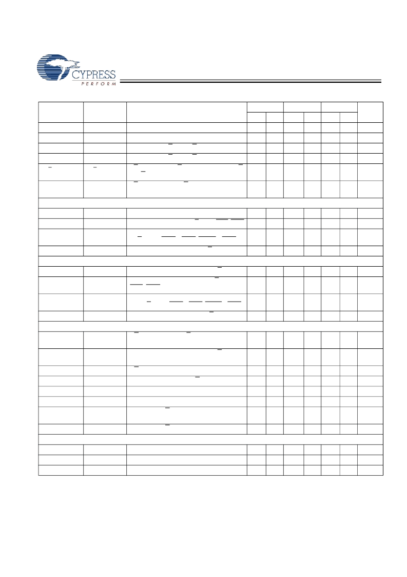
Switching Characteristics
Over the Operating Range
[23, 24]
Cypress
Parameter
t
POWER
t
CYC
t
KH
t
KL
t
KHKH
Consortium
Parameter
Description
250 MHz
Min.
1
4.0
1.6
1.6
1.8
200 MHz
Min.
1
5.0
2.0
2.0
2.2
167 MHz
Min.
1
6.0
2.4
2.4
2.7
Unit
ms
ns
ns
ns
ns
Max
Max
Max
V
DD
(Typical) to the first Access
[25]
K Clock and C Clock Cycle Time
Input Clock (K/K and C/C) HIGH
Input Clock (K/K and C/C) LOW
K/K Clock Rise to K/K Clock Rise and C/C
to C/C Rise (rising edge to rising edge)
K/K Clock Rise to C/C Clock Rise (rising
edge to rising edge)
t
KHKH
t
KHKL
t
KLKH
t
KHKH
6.3
–
–
–
7.9
–
–
–
8.4
–
–
–
t
KHCH
t
KHCH
0.0
1.8
0.0
2.2
0.0
2.7
ns
Set-up Times
t
SA
t
SC
t
SCDDR
t
AVKH
t
IVKH
t
IVKH
Address Set-up to K Clock Rise
Control Set-up to Clock (K, K) Rise (RPS, WPS) 0.35
Double Data Rate Control Set-up to Clock
(K, K) Rise (BWS
0
, BWS
1
, BWS
3
, BWS
4
)
D
[X:0]
Set-up to Clock (K and K) Rise
0.35
–
–
–
0.4
0.4
0.4
–
–
–
0.5
0.5
0.5
–
–
–
ns
ns
ns
0.35
t
SD[26]
Hold Times
t
HA
t
HC
t
DVKH
0.35
–
0.4
–
0.5
–
ns
t
KHAX
t
KHIX
Address Hold after Clock (K and K) Rise
Control Hold after Clock (K and K) Rise
(RPS, WPS)
Double Data Rate Control Hold after Clock
(K and K) Rise (BWS
0
, BWS
1
, BWS
3
, BWS
4
)
D
[X:0]
Hold after Clock (K and K) Rise
0.35
0.35
–
–
0.4
0.4
–
–
0.5
0.5
–
–
ns
ns
t
HCDDR
t
KHIX
0.35
–
0.4
–
0.5
–
ns
t
HD
Output Times
t
CO
t
KHDX
0.35
–
0.4
–
0.5
–
ns
t
CHQV
C/C Clock Rise (or K/K in Single Clock
Mode) to Data Valid
Data Output Hold after Output C/C Clock
Rise (Active to Active)
C/C Clock Rise to Echo Clock Valid
Echo Clock Hold after C/C Clock Rise
Echo Clock High to Data Valid
Echo Clock High to Data Invalid
Clock (C and C) Rise to High-Z (Active to
High-Z)
[27,28]
Clock (C and C) Rise to Low-Z
[27,28]
–
0.45
–
0.45
–
0.50
ns
t
DOH
t
CHQX
–0.45
–
-0.45
–
-0.50
–
ns
t
CCQO
t
CQOH
t
CQD
t
CQDOH
t
CHZ
t
CHCQV
t
CHCQX
t
CQHQV
t
CQHQX
t
CHQZ
–
0.45
–
0.30
–
0.45
–
0.45
–
0.35
–
0.45
–
0.50
–
0.40
–
0.50
ns
ns
ns
ns
ns
–0.45
–
-0.30
–
-0.45
–
-0.35
–
-0.50
–
-0.40
–
t
CLZ
DLL Timing
t
KC Var
t
KC lock
t
KC Reset
Notes:
24.All devices can operate at clock frequencies as low as 119 MHz. When a part with a maximum frequency above 133 MHz is operating at a lower clock frequency,
it requires the input timings of the frequency range in which it is being operated and will output data with the output timings of that frequency range.
25.This part has a voltage regulator internally; t
POWER
is the time that the power needs to be supplied above V
DD
minimum initially before a read or write operation
can be initiated.
26.For D0 data signal on CY7C1525V18 device, t
is 0.5ns for 200MHz, and 250MHz frequencies.
27.t
, t
, are specified with a load capacitance of 5 pF as in part (b) of AC Test Loads. Transition is measured
±
100 mV from steady-state voltage.
28.At any given voltage and temperature t
CHZ
is less than t
CLZ
and t
CHZ
less than t
CO
.
t
CHQX1
-0.45
–
-0.45
–
-0.50
–
ns
t
KC Var
t
KC lock
t
KC Reset
Clock Phase Jitter
DLL Lock Time (K, C)
K Static to DLL Reset
–
0.20
–
–
–
0.20
–
–
–
0.20
–
–
ns
1024
30
1024
30
1024
30
Cycles
ns
[+] Feedback
相關(guān)PDF資料 |
PDF描述 |
|---|---|
| CY7C1510V18-250BZXI | 72-Mbit QDR-II⑩ SRAM 2-Word Burst Architecture |
| CY7C1510V18-278BZC | 72-Mbit QDR-II⑩ SRAM 2-Word Burst Architecture |
| CY7C1510V18-278BZI | 72-Mbit QDR-II⑩ SRAM 2-Word Burst Architecture |
| CY7C1510V18-278BZXC | 72-Mbit QDR-II⑩ SRAM 2-Word Burst Architecture |
| CY7C1510V18-278BZXI | 72-Mbit QDR-II⑩ SRAM 2-Word Burst Architecture |
相關(guān)代理商/技術(shù)參數(shù) |
參數(shù)描述 |
|---|---|
| CY7C15121TC | 制造商:Cypress Semiconductor 功能描述: |
| CY7C15121YC | 制造商:Cypress Semiconductor 功能描述: |
| CY7C15121YC-GBBC | 制造商:Cypress Semiconductor 功能描述: |
| CY7C1512-20VC | 制造商:Cypress Semiconductor 功能描述: |
| CY7C1512-25SC | 制造商:Rochester Electronics LLC 功能描述:- Bulk |
發(fā)布緊急采購,3分鐘左右您將得到回復(fù)。