- 您現(xiàn)在的位置:買賣IC網(wǎng) > PDF目錄379096 > CY7C63310 (Cypress Semiconductor Corp.) enCoRe II Low-Speed USB Peripheral Controller(enCoRe II低速USB外設(shè)控制器) PDF資料下載
參數(shù)資料
| 型號: | CY7C63310 |
| 廠商: | Cypress Semiconductor Corp. |
| 英文描述: | enCoRe II Low-Speed USB Peripheral Controller(enCoRe II低速USB外設(shè)控制器) |
| 中文描述: | enCoRe II還低速USB外設(shè)控制器(enCoRe II還低速的USB外設(shè)控制器) |
| 文件頁數(shù): | 26/74頁 |
| 文件大?。?/td> | 1441K |
| 代理商: | CY7C63310 |
第1頁第2頁第3頁第4頁第5頁第6頁第7頁第8頁第9頁第10頁第11頁第12頁第13頁第14頁第15頁第16頁第17頁第18頁第19頁第20頁第21頁第22頁第23頁第24頁第25頁當(dāng)前第26頁第27頁第28頁第29頁第30頁第31頁第32頁第33頁第34頁第35頁第36頁第37頁第38頁第39頁第40頁第41頁第42頁第43頁第44頁第45頁第46頁第47頁第48頁第49頁第50頁第51頁第52頁第53頁第54頁第55頁第56頁第57頁第58頁第59頁第60頁第61頁第62頁第63頁第64頁第65頁第66頁第67頁第68頁第69頁第70頁第71頁第72頁第73頁第74頁
CY7C63310
CY7C638xx
Document 38-08035 Rev. *I
Page 26 of 74
12.0
Sleep Mode
The CPU can only be put to sleep by the firmware. This is
accomplished by setting the Sleep bit in the System Status and
Control Register (CPU_SCR). This stops the CPU from
executing instructions, and the CPU will remain asleep until an
interrupt comes pending, or there is a reset event (either a
Power-on Reset, or a Watchdog Timer Reset).
The Low-voltage Detection circuit (LVD) drops into fully
functional power-reduced states, and the latency for the LVD
is increased. The actual latency can be traded against power
consumption by changing Sleep Duty Cycle field of the
ECO_TR Register.
The Internal 32 KHz Low-speed Oscillator remains running.
Prior to entering suspend mode, firmware can optionally
configure the 32 KHz Low-speed Oscillator to operate in a low-
power mode to help reduce the over all power consumption
(Using Bit 7,
Table 10-2
). This will help save approximately
5
μ
A; however, the trade off is that the 32 KHz Low-speed
Oscillator will be less accurate.
All interrupts remain active. Only the occurrence of an interrupt
will wake the part from sleep. The Stop bit in the System Status
and Control Register (CPU_SCR) must be cleared for a part
to resume out of sleep. The Global Interrupt Enable bit of the
CPU Flags Register (CPU_F) does not have any effect. Any
unmasked interrupt will wake the system up. As a result, any
interrupts not intended for waking must be disabled through
the Interrupt Mask Registers.
When the CPU enters sleep mode the CPUCLK Select (Bit 1,
Table 10-3
) is forced to the Internal Oscillator. The internal
oscillator recovery time is three clock cycles of the Internal 32
KHz Low-power Oscillator. The Internal 24 MHz Oscillator
restarts immediately on exiting Sleep mode. If an external
clock is used, firmware will need to switch the clock source for
the CPU.
On exiting sleep mode, once the clock is stable and the delay
time has expired, the instruction immediately following the
sleep instruction is executed before the interrupt service
routine (if enabled).
The Sleep interrupt allows the microcontroller to wake up
periodically and poll system components while maintaining
very low average power consumption. The Sleep interrupt
may also be used to provide periodic interrupts during non-
sleep modes.
12.1
The SLEEP bit is an input into the sleep logic circuit. This
circuit is designed to sequence the device into and out of the
hardware sleep state. The hardware sequence to put the
device to sleep is shown in
Figure 12-1
and is defined as
follows.
1.Firmware sets the SLEEP bit in the CPU_SCR0 register. The
Bus Request (BRQ) signal to the CPU is immediately
asserted. This is a request by the system to halt CPU
operation at an instruction boundary. The CPU samples BRQ
on the positive edge of CPUCLK.
2.Due to the specific timing of the register write, the CPU
issues a Bus Request Acknowledge (BRA) on the following
positive edge of the CPU clock. The sleep logic waits for the
following negative edge of the CPU clock and then asserts a
system-wide Power Down (PD) signal. In
Figure 12-1
the CPU
is halted and the system-wide power down signal is asserted.
3.The system-wide PD (power down) signal controls several
major circuit blocks: The Flash memory module, the internal
24 MHz oscillator, the EFTB filter and the bandgap voltage
reference. These circuits transition into a zero power state.
The only operational circuits on chip are the Low Power oscil-
lator, the bandgap refresh circuit, and the supply voltage
monitor (POR/LVD) circuit.
Note:
To achieve the lowest possible power consumption
during suspend/sleep, the following conditions must be
observed in addition to considerations for the sleep timer:
All GPIOs must be set to outputs and driven low
The USB pins P1.0 and P1.1 should be configured as inputs
with their pull-ups enabled.
Sleep Sequence
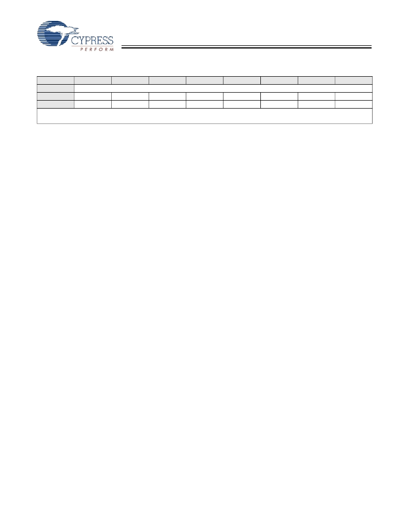
Table 11-2. Reset Watchdog Timer (RESWDT) [0xE3] [W]
Bit #
7
6
5
4
3
2
1
0
Field
Reset Watchdog Timer [7:0]
Read/Write
W
W
W
W
W
W
W
W
Default
0
0
0
0
0
0
0
0
Any write to this register will clear Watchdog Timer, a write of 0x38 will also clear the Sleep Timer
Bit [7:0]:
Reset Watchdog Timer [7:0]
相關(guān)PDF資料 |
PDF描述 |
|---|---|
| CY7C63801 | enCoRe II Low-Speed USB Peripheral Controller(enCoRe II低速USB外設(shè)控制器) |
| CY7C63823 | enCoRe II Low-Speed USB Peripheral Controller(enCoRe II低速USB外設(shè)控制器) |
| CY7C63813 | enCoRe II Low-Speed USB Peripheral Controller(enCoRe II低速USB外設(shè)控制器) |
| CY7C63833 | enCoRe II Low-Speed USB Peripheral Controller(enCoRe II低速USB外設(shè)控制器) |
| CY7C65640-LFXC | TetraHub High-speed USB Hub Controller |
相關(guān)代理商/技術(shù)參數(shù) |
參數(shù)描述 |
|---|---|
| CY7C63310-PXC | 功能描述:USB 接口集成電路 USB 3K Flash 128 byte RAM COM RoHS:否 制造商:Cypress Semiconductor 產(chǎn)品:USB 2.0 數(shù)據(jù)速率: 接口類型:SPI 工作電源電壓:3.15 V to 3.45 V 工作電源電流: 最大工作溫度:+ 85 C 安裝風(fēng)格:SMD/SMT 封裝 / 箱體:WLCSP-20 |
| CY7C63310-SXC | 功能描述:USB 接口集成電路 USB Peripheral Cntrl 3K/128 16-SOIC RoHS:否 制造商:Cypress Semiconductor 產(chǎn)品:USB 2.0 數(shù)據(jù)速率: 接口類型:SPI 工作電源電壓:3.15 V to 3.45 V 工作電源電流: 最大工作溫度:+ 85 C 安裝風(fēng)格:SMD/SMT 封裝 / 箱體:WLCSP-20 |
| CY7C63310-SXCES | 制造商:Cypress Semiconductor 功能描述: |
| CY7C634121C-PVXC | 制造商:Cypress Semiconductor 功能描述: |
| CY7C634121C-PXC | 制造商:Cypress Semiconductor 功能描述: |
發(fā)布緊急采購,3分鐘左右您將得到回復(fù)。