- 您現(xiàn)在的位置:買賣IC網(wǎng) > PDF目錄379096 > CY7C63823 (Cypress Semiconductor Corp.) enCoRe II Low-Speed USB Peripheral Controller(enCoRe II低速USB外設(shè)控制器) PDF資料下載
參數(shù)資料
| 型號: | CY7C63823 |
| 廠商: | Cypress Semiconductor Corp. |
| 英文描述: | enCoRe II Low-Speed USB Peripheral Controller(enCoRe II低速USB外設(shè)控制器) |
| 中文描述: | enCoRe II還低速USB外設(shè)控制器(enCoRe II還低速的USB外設(shè)控制器) |
| 文件頁數(shù): | 30/74頁 |
| 文件大?。?/td> | 1441K |
| 代理商: | CY7C63823 |
第1頁第2頁第3頁第4頁第5頁第6頁第7頁第8頁第9頁第10頁第11頁第12頁第13頁第14頁第15頁第16頁第17頁第18頁第19頁第20頁第21頁第22頁第23頁第24頁第25頁第26頁第27頁第28頁第29頁當前第30頁第31頁第32頁第33頁第34頁第35頁第36頁第37頁第38頁第39頁第40頁第41頁第42頁第43頁第44頁第45頁第46頁第47頁第48頁第49頁第50頁第51頁第52頁第53頁第54頁第55頁第56頁第57頁第58頁第59頁第60頁第61頁第62頁第63頁第64頁第65頁第66頁第67頁第68頁第69頁第70頁第71頁第72頁第73頁第74頁
CY7C63310
CY7C638xx
Document 38-08035 Rev. *I
Page 30 of 74
13.0.1
ECO Trim Register
14.0
General-purpose I/O Ports
14.1
Port Data Registers
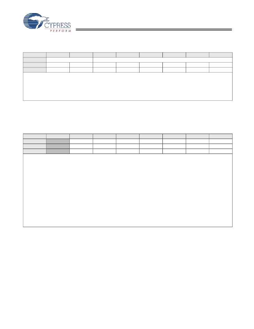
Table 13-3. ECO (ECO_TR) [0x1EB] [R/W]
Bit #
7
6
5
4
3
2
1
0
Field
Sleep Duty Cycle [1:0]
Reserved
Read/Write
R/W
R/W
–
–
–
–
–
–
Default
0
0
0
0
0
0
0
0
This register controls the ratios (in numbers of 32-KHz clock periods) of “on” time versus “off” time for LVD and POR detection
circuit
Bit [7:6]:
Sleep Duty Cycle [1:0]
0 0 = 128 periods of the Internal 32 KHz Low-speed Oscillator
0 1 = 512 periods of the Internal 32 KHz Low-speed Oscillator
1 0 = 32 periods of the Internal 32 KHz Low-speed Oscillator
1 1 = 8 periods of the Internal 32 KHz Low-speed Oscillator
Table 14-1. P0 Data Register (P0DATA)[0x00] [R/W]
Bit #
7
6
5
4
3
2
1
0
Field
P0.7
P0.6/TIO1
P0.5/TIO0
P0.4/INT2
P0.3/INT1
P0.2/INT0
P0.1/CLKOUT
P0.0/CLKIN
Read/Write
R/W
R/W
R/W
R/W
R/W
R/W
R/W
R/W
Default
0
0
0
0
0
0
0
0
This register contains the data for Port 0. Writing to this register sets the bit values to be output on output enabled pins. Reading
from this register returns the current state of the Port 0 pins.
Bit 7:
P0.7 Data
P0.7 only exists in the CY7C638xx
Bit [6:5]:
P0.6–P0.5 Data/TIO1 and TIO0
Beside their use as the P0.6–P0.5 GPIOs, these pins can also be used for the alternate functions as the Capture Timer input or
Timer output pins (TIO1 and TIO0). To configure the P0.5 and P0.6 pins, refer to the P0.5/TIO0–P0.6/TIO1 Configuration Register
(
Table 14-8
)
The use of the pins as the P0.6–P0.5 GPIOs and the alternate functions exist in all the enCoRe II parts
Bit [4:2]:
P0.4–P0.2 Data/INT2 – INT0
Beside their use as the P0.4–P0.2 GPIOs, these pins can also be used for the alternate functions as the Interrupt pins
(INT0–INT2). To configure the P0.4–P0.2 pins, refer to the P0.2/INT0–P0.4/INT2 Configuration Register (
Table 14-7
)
The use of the pins as the P0.4–P0.2 GPIOs and the alternate functions exist in all the enCoRe II parts
Bit 1:
P0.1/CLKOUT
Beside its use as the P0.1 GPIO, this pin can also be used for the alternate function as the CLK OUT pin. To configure the P0.1
pin, refer to the P0.1/CLKOUT Configuration Register (
Table 14-6
)
Bit 0:
P0.0/CLKIN
Beside its use as the P0.0 GPIO, this pin can also be used for the alternate function as the CLKIN pin. To configure the P0.0
pin, refer to the P0.0/CLKIN Configuration Register (
Table 14-5
)
相關(guān)PDF資料 |
PDF描述 |
|---|---|
| CY7C63813 | enCoRe II Low-Speed USB Peripheral Controller(enCoRe II低速USB外設(shè)控制器) |
| CY7C63833 | enCoRe II Low-Speed USB Peripheral Controller(enCoRe II低速USB外設(shè)控制器) |
| CY7C65640-LFXC | TetraHub High-speed USB Hub Controller |
| CY7C65640 | TetraHub High-speed USB Hub Controller |
| CY7C65640-LFC | TetraHub High-speed USB Hub Controller |
相關(guān)代理商/技術(shù)參數(shù) |
參數(shù)描述 |
|---|---|
| CY7C63823-3XWC | 制造商:Cypress Semiconductor 功能描述:USB - Bulk 制造商:Cypress Semiconductor 功能描述:Bulk / USB Low-Speed Peripherals |
| CY7C638234-SXC | 功能描述:IC USB CONTROLLERS RoHS:是 類別:集成電路 (IC) >> 接口 - 控制器 系列:- 標準包裝:4,900 系列:- 控制器類型:USB 2.0 控制器 接口:串行 電源電壓:3 V ~ 3.6 V 電流 - 電源:135mA 工作溫度:0°C ~ 70°C 安裝類型:表面貼裝 封裝/外殼:36-VFQFN 裸露焊盤 供應(yīng)商設(shè)備封裝:36-QFN(6x6) 包裝:* 其它名稱:Q6396337A |
| CY7C638235-SXC | 制造商:Rochester Electronics LLC 功能描述: 制造商:Cypress Semiconductor 功能描述: |
| CY7C63823-PXC | 功能描述:IC USB PERIPHERAL CTRLR 24-DIP RoHS:是 類別:集成電路 (IC) >> 接口 - 控制器 系列:CY7C 標準包裝:4,900 系列:- 控制器類型:USB 2.0 控制器 接口:串行 電源電壓:3 V ~ 3.6 V 電流 - 電源:135mA 工作溫度:0°C ~ 70°C 安裝類型:表面貼裝 封裝/外殼:36-VFQFN 裸露焊盤 供應(yīng)商設(shè)備封裝:36-QFN(6x6) 包裝:* 其它名稱:Q6396337A |
| CY7C63823-QXC | 功能描述:USB 接口集成電路 USB Peripheral Cntrl 8K/256 24-QSOP RoHS:否 制造商:Cypress Semiconductor 產(chǎn)品:USB 2.0 數(shù)據(jù)速率: 接口類型:SPI 工作電源電壓:3.15 V to 3.45 V 工作電源電流: 最大工作溫度:+ 85 C 安裝風格:SMD/SMT 封裝 / 箱體:WLCSP-20 |
發(fā)布緊急采購,3分鐘左右您將得到回復(fù)。