- 您現(xiàn)在的位置:買賣IC網(wǎng) > PDF目錄379096 > CY7C63833 (Cypress Semiconductor Corp.) enCoRe II Low-Speed USB Peripheral Controller(enCoRe II低速USB外設(shè)控制器) PDF資料下載
參數(shù)資料
| 型號: | CY7C63833 |
| 廠商: | Cypress Semiconductor Corp. |
| 英文描述: | enCoRe II Low-Speed USB Peripheral Controller(enCoRe II低速USB外設(shè)控制器) |
| 中文描述: | enCoRe II還低速USB外設(shè)控制器(enCoRe II還低速的USB外設(shè)控制器) |
| 文件頁數(shù): | 46/74頁 |
| 文件大小: | 1441K |
| 代理商: | CY7C63833 |
第1頁第2頁第3頁第4頁第5頁第6頁第7頁第8頁第9頁第10頁第11頁第12頁第13頁第14頁第15頁第16頁第17頁第18頁第19頁第20頁第21頁第22頁第23頁第24頁第25頁第26頁第27頁第28頁第29頁第30頁第31頁第32頁第33頁第34頁第35頁第36頁第37頁第38頁第39頁第40頁第41頁第42頁第43頁第44頁第45頁當(dāng)前第46頁第47頁第48頁第49頁第50頁第51頁第52頁第53頁第54頁第55頁第56頁第57頁第58頁第59頁第60頁第61頁第62頁第63頁第64頁第65頁第66頁第67頁第68頁第69頁第70頁第71頁第72頁第73頁第74頁
CY7C63310
CY7C638xx
Document 38-08035 Rev. *I
Page 46 of 74
17.0
Interrupt Controller
The interrupt controller and its associated registers allow the
user’s code to respond to an interrupt from almost every
functional block in the enCoRe II devices. The registers
associated with the interrupt controller allow interrupts to be
disabled either globally or individually. The registers also
provide a mechanism by which a user may clear all pending
and posted interrupts, or clear individual posted or pending
interrupts.
The following table lists all interrupts and the priorities that are
available in the enCoRe II devices.
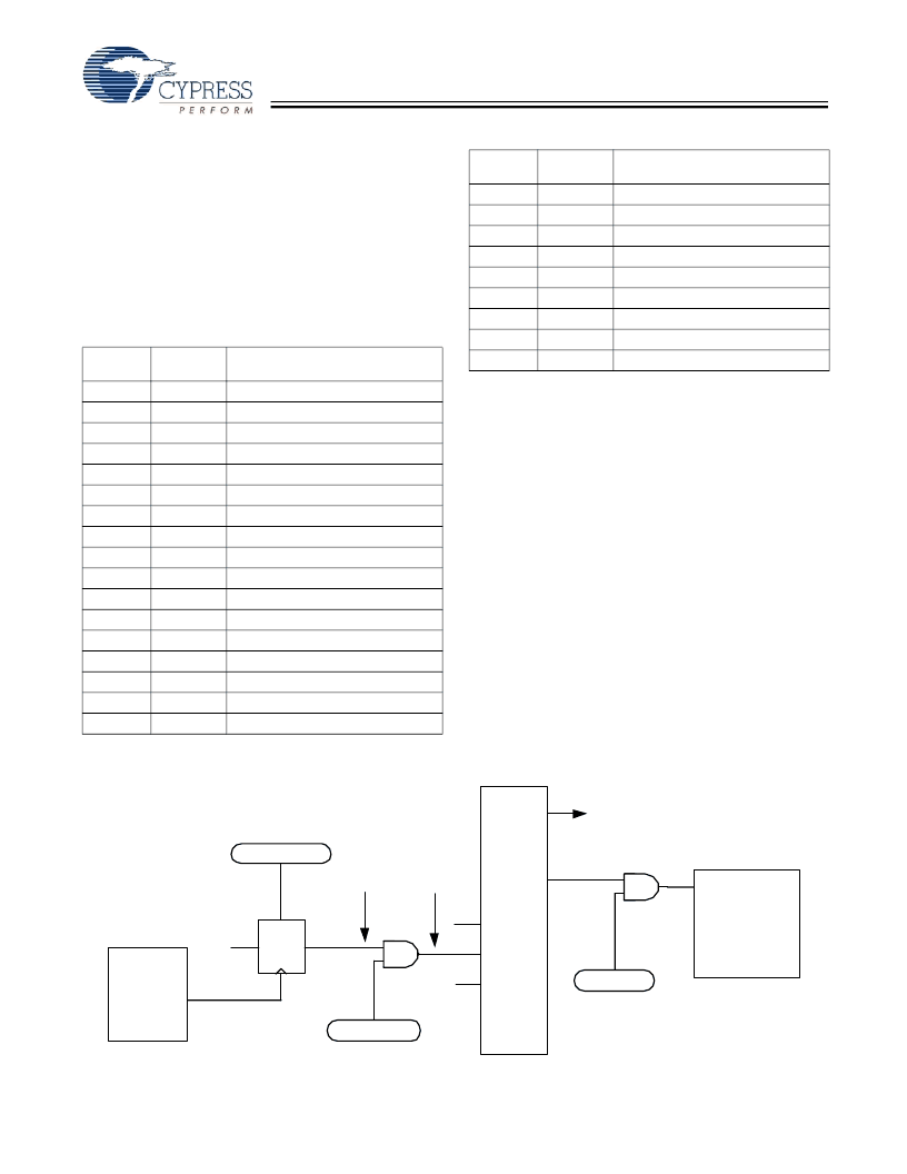
17.1
An interrupt is posted when its interrupt conditions occur. This
results in the flip-flop in
Figure 17-1
clocking in a ‘1’. The
interrupt will remain posted until the interrupt is taken or until
it is cleared by writing to the appropriate INT_CLRx register.
A posted interrupt is not pending unless it is enabled by setting
its interrupt mask bit (in the appropriate INT_MSKx register).
All pending interrupts are processed by the Priority Encoder to
determine the highest priority interrupt which will be taken by
the M8C if the Global Interrupt Enable bit is set in the CPU_F
register.
Disabling an interrupt by clearing its interrupt mask bit (in the
INT_MSKx register) does not clear a posted interrupt, nor
does it prevent an interrupt from being posted. It simply
prevents a posted interrupt from becoming pending.
Nested interrupts can be accomplished by re-enabling inter-
rupts inside an interrupt service routine. To do this, set the IE
bit in the Flag Register.
A block diagram of the enCoRe II Interrupt Controller is shown
in
Figure 17-1
.
Architectural Description
Table 17-1. Interrupt Numbers, Priorities, Vectors
Interrupt
Priority
0
1
2
3
4
5
6
7
8
9
10
11
12
13
14
15
16
Interrupt
Address
0000h
0004h
0008h
000Ch
0010h
0014h
0018h
001Ch
0020h
0024h
0028h
002Ch
0030h
0034h
0038h
003Ch
0040h
Name
Reset
POR/LVD
INT0
SPI Transmitter Empty
SPI Receiver Full
GPIO Port 0
GPIO Port 1
INT1
EP0
EP1
EP2
USB Reset
USB Active
1 mS Interval timer
Programmable Interval Timer
Timer Capture 0
Timer Capture 1
17
18
19
20
21
22
23
24
25
0044h
0048h
004Ch
0050h
0054h
0058h
005Ch
0060h
0064h
16-bit Free Running Timer Wrap
INT2
PS2 Data Low
GPIO Port 2
GPIO Port 3
Reserved
Reserved
Reserved
Sleep Timer
Table 17-1. Interrupt Numbers, Priorities, Vectors
(contin-
Interrupt
Priority
Interrupt
Address
Name
Figure 17-1. Interrupt Controller Block Diagram
Interrupt
Source
(Timer,
GPIO, etc.)
Interrupt Taken
or
INT_CLRx Write
Posted
Interrupt
Pending
Interrupt
GIE
Interrupt Vector
Mask Bit Setting
D
R
Q
1
Priority
Encoder
M8C Core
Interrupt
Request
.
.
INT_MSKx
CPU_F[0]
相關(guān)PDF資料 |
PDF描述 |
|---|---|
| CY7C65640-LFXC | TetraHub High-speed USB Hub Controller |
| CY7C65640 | TetraHub High-speed USB Hub Controller |
| CY7C65640-LFC | TetraHub High-speed USB Hub Controller |
| CY4602 | TetraHub High-speed USB Hub Controller |
| CY7C65640A | TetraHub High-Speed USB Hub Controller(TetraHub高速USB Hub控制器) |
相關(guān)代理商/技術(shù)參數(shù) |
參數(shù)描述 |
|---|---|
| CY7C638334-LTXC | 制造商:Cypress Semiconductor 功能描述: |
| CY7C638335-LFXC | 制造商:Cypress Semiconductor 功能描述: |
| CY7C638335-LTXC | 制造商:Cypress Semiconductor 功能描述: |
| CY7C63833-LFXC | 功能描述:USB 接口集成電路 8K Flash 256 byte RAM COM RoHS:否 制造商:Cypress Semiconductor 產(chǎn)品:USB 2.0 數(shù)據(jù)速率: 接口類型:SPI 工作電源電壓:3.15 V to 3.45 V 工作電源電流: 最大工作溫度:+ 85 C 安裝風(fēng)格:SMD/SMT 封裝 / 箱體:WLCSP-20 |
| CY7C63833-LTXC | 功能描述:USB 接口集成電路 USB Peripheral Cntrl 8K/256 32-QFN RoHS:否 制造商:Cypress Semiconductor 產(chǎn)品:USB 2.0 數(shù)據(jù)速率: 接口類型:SPI 工作電源電壓:3.15 V to 3.45 V 工作電源電流: 最大工作溫度:+ 85 C 安裝風(fēng)格:SMD/SMT 封裝 / 箱體:WLCSP-20 |
發(fā)布緊急采購,3分鐘左右您將得到回復(fù)。