- 您現(xiàn)在的位置:買賣IC網(wǎng) > PDF目錄379152 > DL202 (Electronics Industry Public Company Limited) SILICON RECTIFIER DIODES PDF資料下載
參數(shù)資料
| 型號: | DL202 |
| 廠商: | Electronics Industry Public Company Limited |
| 英文描述: | SILICON RECTIFIER DIODES |
| 中文描述: | 一般整流二極管 |
| 文件頁數(shù): | 1/2頁 |
| 文件大小: | 51K |
| 代理商: | DL202 |
DL200 - DL210
SILICON RECTIFIER DIODES
PRV : 50 - 1000 Volts
Io : 2.0 Amperes
FEATURES :
* High current capability
* High surge current capability
* High reliability
* Low reverse current
* Low forward voltage drop
* Pb / RoHS Free
MECHANICAL DATA :
* Case : D2 Molded plastic
* Epoxy : UL94V-O rate flame retardant
* Lead : Axial lead solderable per MIL-STD-202,
Method 208 guaranteed
* Polarity : Color band denotes cathode end
* Mounting position : Any
* Weight : 0.465 gram
MAXIMUM RATINGS AND ELECTRICAL CHARACTERISTICS
Rating at 25
°
C ambient temperature unless otherwise specified.
Single phase, half wave, 60 Hz, resistive or inductive load.
For capacitive load, derate current by 20%.
SYMBOL
DL201
DL202
DL203
DL204
DL205
DL206
DL207
UNIT
Maximum Repetitive Peak Reverse Voltage
Maximum RMS Voltage
Maximum DC Blocking Voltage
Maximum Average Forward Current
0.375"(9.5mm) Lead Length Ta = 50
°
C
Peak Forward Surge Current
8.3ms Single half sine wave Superimposed
on rated load (JEDEC Method)
Maximum Forward Voltage at I
F
= 2.0 Amps.
Maximum DC Reverse Current Ta = 25
°
C
at rated DC Blocking Voltage Ta = 100
°
C
Typical Junction Capacitance (Note1)
Typical Thermal Resistance (Note2)
Junction Temperature Range
Storage Temperature Range
V
RRM
V
RMS
V
DC
50
35
50
100
70
100
200
140
200
400
280
400
600
420
600
800
560
800
1000
700
1000
V
V
V
V
F
I
R
I
R(H)
C
J
R
θ
JA
T
J
T
STG
1.0
5.0
50
75
20
V
μ
A
μ
A
pF
°
C/W
°
C
°
C
- 65 to + 175
- 65 to + 175
Notes :
(1) Measured at 1.0 MHz and applied reverse voltage of 4.0V
DC
(2) Thermal resistance from Junction to Ambient at 0.375" (9.5mm) Lead Lengths, P.C. Board Mounted.
Page 1 of 2
Rev. 02 : March 25, 2005
RATING
A
A
2.0
I
F
I
FSM
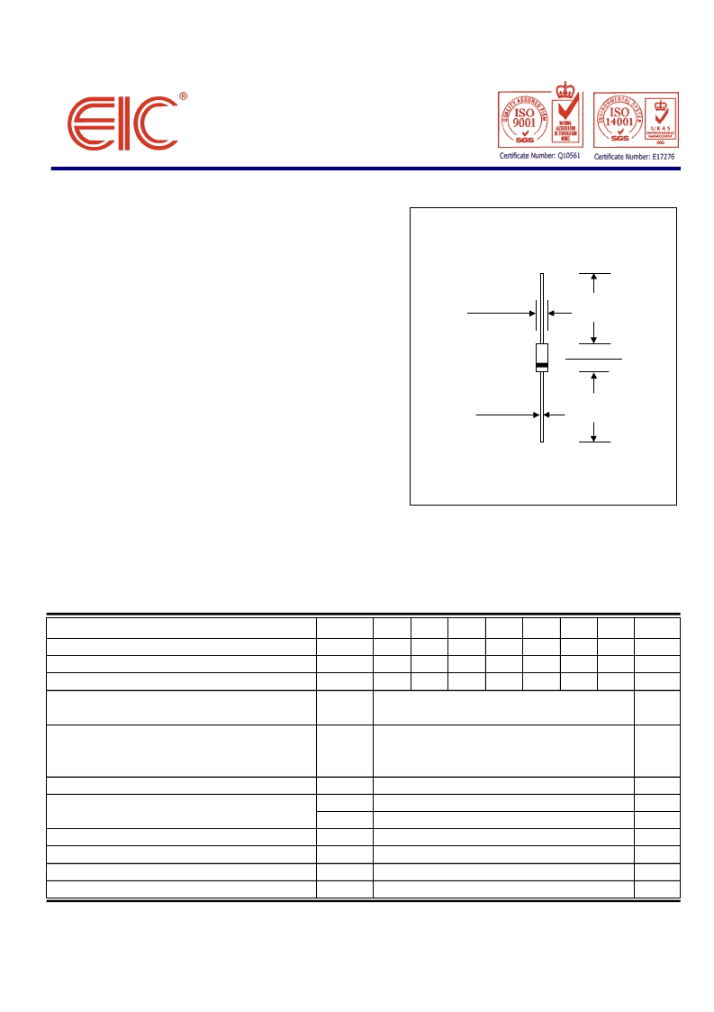
75
0.034 (0.86)
0.028 (0.71)
D2
0.161 (4.10)
0.154 (3.90)
Dimensions in inches and ( mllimeters )
0.284 (7.20)
0.268 (6.84)
1.00 (25.4)
MIN.
1.00 (25.4)
MIN.
相關PDF資料 |
PDF描述 |
|---|---|
| DL203 | SILICON RECTIFIER DIODES |
| DL204 | SILICON RECTIFIER DIODES |
| DL205 | SILICON RECTIFIER DIODES |
| DL206 | SILICON RECTIFIER DIODES |
| DL330M | Optoelectronic |
相關代理商/技術參數(shù) |
參數(shù)描述 |
|---|---|
| DL20224693-C26 | 制造商:MACHINE SCREWS 功能描述: |
| DL20224693-C3 | 制造商:MACHINE SCREWS 功能描述: |
| DL20224693-C7 | 制造商:MACHINE SCREWS 功能描述: |
| DL2025 | 制造商:DURACELL 功能描述:Bulk |
| DL20251957-15 | 制造商:MACHINE SCREWS 功能描述: |
發(fā)布緊急采購,3分鐘左右您將得到回復。