- 您現(xiàn)在的位置:買賣IC網(wǎng) > PDF目錄353067 > DP83932CVF33 LAN Node Controller PDF資料下載
參數(shù)資料
| 型號: | DP83932CVF33 |
| 英文描述: | LAN Node Controller |
| 中文描述: | 網(wǎng)絡(luò)節(jié)點控制器 |
| 文件頁數(shù): | 22/24頁 |
| 文件大?。?/td> | 240K |
| 代理商: | DP83932CVF33 |
50 Functional Description
This section describes the three major blocks of the
DP83957 These are the
1) SRAM Interface
2) Management Interface
3) CPU Interface
51 SRAM INTERFACE
The DP83957 interfaces directly with standard off-the-shelf
1kx8or2kx8 fast SRAM without any additional buffering
The DP83957 can support access times of 25 ns and 45 ns
If one DP839502 is used then a minimum 1k x 8 SRAM is
required
If two DP839502’s are used (on a shared management
bus) then a minimum 2k x 8 SRAM is required
The SRAM connected to the DP83957 stores the Manage-
ment Information Base (MIB) attributes that are extracted
from the DP83950’s management bus
The SRAM Interface consists of the following pins
SRA 130
14-Bit Address Lines
SRD 70
8-Bit Data Bus
SRWR
Write Enable
SROE
Output Enable
The SRAM interface does not include a chip select output to
enable the SRAM
as the SRAM is dedicated to the
DP83957 Therefore the SRAM’s chip select input must al-
ways be enabled
511 SRAM Configuration
The DP83957 must be configured correctly to allow it to
interface with the SRAM This is achieved through Configu-
ration Registers 1 and 2 (refer to Sections 62 and 63 for a
description of these registers)
The access time of the SRAM can be specified through the
SRAM
ACC bit (D4) of Configuration Register 2
If bit D4 e 0 then a SRAM access time of 25 ns is selected
If bit D4 e 1 then an access time of between 25 ns and
45 ns is selected
The size of the SRAM must also be specified through the
SIZE bit (D3) of Configuration Register 2 If bit D3 e 0 then
a1kx8is selected If bit D3 e 1 thena2kx8is selected
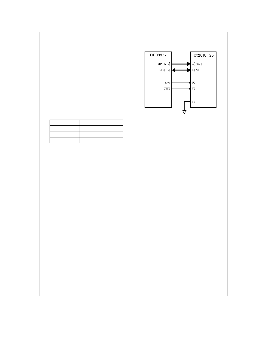
The following diagram shows the external SRAM connec-
tion to the DP83957
TLF12437 – 4
External SRAM Connection to DP83957
512 SRAM Read Operation
A read of the SRAM can occur due to a CPU request for one
of the PORT attributes or due to normal updating of attri-
butes by the DP83957 after receiving the management sta-
tistics from the DP83950
In the latter case the access to the SRAM is achieved auto-
matically by the DP83957 In the case of a CPU request the
SRAM address must be specified in Access Registers 1 and
2 (refer to Sections 68 and 69)
The REP
SEL bit (D4) of Access Register 2 specifies the
DP83950 ID and the PORT
ID bits (D 30 ) specify the
PORT ID Together they select the SRAM page The offset
within the page ie the attributes is specified through Ac-
cess Register 1 The ACC
50 bits (D 50 ) specify the
attribute (offset) to be read (Refer to Section 515 SRAM
Address Format)
The DP83957 can read data from the SRAM in variable byte
lengths The number of bytes to be read is specified through
bits D 02 of Configuration Register 1 The DP83957 can
read up to 6 bytes from the SRAM at any one time The data
that is read from the SRAM is placed in Read Data Regis-
ters 1 – 6
The CPU initiates an SRAM read by setting the ST-RD bit
(D4) of Configuration Register 1 The DP83957 resets this
bit after the read has completed It also indicates comple-
tion of the SRAM read operation by sending an interrupt (if
enabled) to the CPU and setting RD
COM bit (D4) of the
Interrupt Status Register
7
相關(guān)PDF資料 |
PDF描述 |
|---|---|
| DP83934 | |
| DP83934AVQB | LAN Node Controller |
| DP83934CVUL20 | LAN Node Controller |
| DP83934CVUL25 | LAN Node Controller |
| DP83936AVUL20 | LAN Node Controller |
相關(guān)代理商/技術(shù)參數(shù) |
參數(shù)描述 |
|---|---|
| DP83932CVF-33 | 制造商:Rochester Electronics LLC 功能描述:- Bulk |
| DP83934 | 制造商:未知廠家 制造商全稱:未知廠家 功能描述: |
| DP83934AVQB | 功能描述:IC CTRLR ORIENT NETWORK 160PLCC RoHS:否 類別:集成電路 (IC) >> 接口 - 控制器 系列:- 標(biāo)準(zhǔn)包裝:4,900 系列:- 控制器類型:USB 2.0 控制器 接口:串行 電源電壓:3 V ~ 3.6 V 電流 - 電源:135mA 工作溫度:0°C ~ 70°C 安裝類型:表面貼裝 封裝/外殼:36-VFQFN 裸露焊盤 供應(yīng)商設(shè)備封裝:36-QFN(6x6) 包裝:* 其它名稱:Q6396337A |
| DP83934AVQB WAF | 制造商:Texas Instruments 功能描述: |
| DP83934CVUL20 | 制造商:未知廠家 制造商全稱:未知廠家 功能描述:LAN Node Controller |
發(fā)布緊急采購,3分鐘左右您將得到回復(fù)。