- 您現(xiàn)在的位置:買賣IC網(wǎng) > PDF目錄362737 > EP1C6T144I7 (Altera Corporation) Cyclone FPGA Family PDF資料下載
參數(shù)資料
| 型號(hào): | EP1C6T144I7 |
| 廠商: | Altera Corporation |
| 英文描述: | Cyclone FPGA Family |
| 中文描述: | 氣旋FPGA系列 |
| 文件頁(yè)數(shù): | 52/94頁(yè) |
| 文件大小: | 1138K |
| 代理商: | EP1C6T144I7 |
第1頁(yè)第2頁(yè)第3頁(yè)第4頁(yè)第5頁(yè)第6頁(yè)第7頁(yè)第8頁(yè)第9頁(yè)第10頁(yè)第11頁(yè)第12頁(yè)第13頁(yè)第14頁(yè)第15頁(yè)第16頁(yè)第17頁(yè)第18頁(yè)第19頁(yè)第20頁(yè)第21頁(yè)第22頁(yè)第23頁(yè)第24頁(yè)第25頁(yè)第26頁(yè)第27頁(yè)第28頁(yè)第29頁(yè)第30頁(yè)第31頁(yè)第32頁(yè)第33頁(yè)第34頁(yè)第35頁(yè)第36頁(yè)第37頁(yè)第38頁(yè)第39頁(yè)第40頁(yè)第41頁(yè)第42頁(yè)第43頁(yè)第44頁(yè)第45頁(yè)第46頁(yè)第47頁(yè)第48頁(yè)第49頁(yè)第50頁(yè)第51頁(yè)當(dāng)前第52頁(yè)第53頁(yè)第54頁(yè)第55頁(yè)第56頁(yè)第57頁(yè)第58頁(yè)第59頁(yè)第60頁(yè)第61頁(yè)第62頁(yè)第63頁(yè)第64頁(yè)第65頁(yè)第66頁(yè)第67頁(yè)第68頁(yè)第69頁(yè)第70頁(yè)第71頁(yè)第72頁(yè)第73頁(yè)第74頁(yè)第75頁(yè)第76頁(yè)第77頁(yè)第78頁(yè)第79頁(yè)第80頁(yè)第81頁(yè)第82頁(yè)第83頁(yè)第84頁(yè)第85頁(yè)第86頁(yè)第87頁(yè)第88頁(yè)第89頁(yè)第90頁(yè)第91頁(yè)第92頁(yè)第93頁(yè)第94頁(yè)
52
Altera Corporation
Cyclone FPGA Family Data Sheet
Preliminary Information
DDR SDRAM & FCRAM
Cyclone devices have dedicated circuitry for interfacing with DDR
SDRAM. All I/O banks support DDR SDRAM and FCRAM I/O pins.
However, the configuration input pins in bank 1 must operate at 2.5 V
because the SSTL-2 V
CCIO
level is 2.5 V. Additionally, the configuration
output pins (
nSTATUS
and
CONF_DONE
) and all the JTAG pins in I/O
bank 3 must operate at 2.5 V because the V
CCIO
level of SSTL-2 is 2.5 V.
I/O banks 1, 2, 3, and 4 support DQS signals with DQ bus modes of
×
8.
For
×
8 mode, there are up to eight groups of programmable DQS and DQ
pins, I/O banks 1, 2, 3, and 4 each have two groups in the 324-pin and
400-pin FineLine BGA packages. Each group consists of one DQS pin, a set
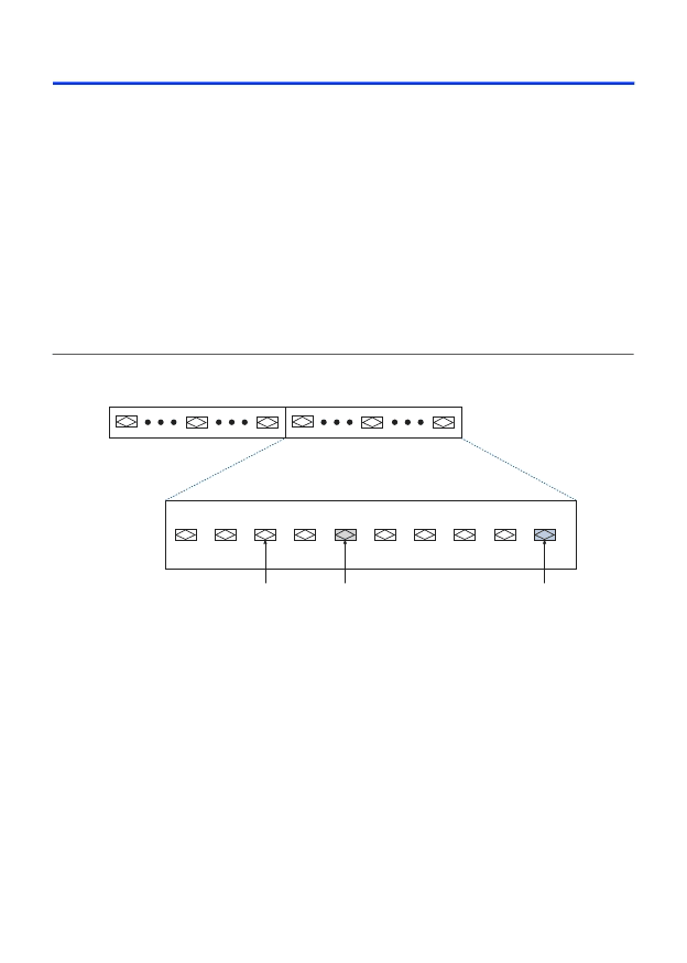
of eight DQ pins, and one DM pin (see
Figure 33
). Each DQS pin drives the
set of eight DQ pins within that group.
Figure 33. Cyclone Device DQ & DQS Groups in
×
8 Mode
Note (1)
Note to
Figure 33
:
(1)
Each DQ group consists of one DQS pin, eight DQ pins, and one DM pin.
DQ Pins
DQS Pin
DM Pin
Top, Bottom, Left, or Right I/O Bank
相關(guān)PDF資料 |
PDF描述 |
|---|---|
| EP1C6T144I8 | Cyclone FPGA Family |
| EP1C6T240C6 | Cyclone FPGA Family |
| EP1C6T240C7 | Cyclone FPGA Family |
| EP1C6T240C8 | Cyclone FPGA Family |
| EP1C6T240I6 | Cyclone FPGA Family |
相關(guān)代理商/技術(shù)參數(shù) |
參數(shù)描述 |
|---|---|
| EP1C6T144I7N | 功能描述:FPGA - 現(xiàn)場(chǎng)可編程門陣列 FPGA - Cyclone I 598 LABs 98 IOs RoHS:否 制造商:Altera Corporation 系列:Cyclone V E 柵極數(shù)量: 邏輯塊數(shù)量:943 內(nèi)嵌式塊RAM - EBR:1956 kbit 輸入/輸出端數(shù)量:128 最大工作頻率:800 MHz 工作電源電壓:1.1 V 最大工作溫度:+ 70 C 安裝風(fēng)格:SMD/SMT 封裝 / 箱體:FBGA-256 |
| EP1F | 制造商:NEC 制造商全稱:NEC 功能描述:HIGH HEAT RESISTIVITY |
| EP1F-B3G1 | 制造商:NEC 制造商全稱:NEC 功能描述:HIGH HEAT RESISTIVITY |
| EP1FB3G1S | 制造商:World Products 功能描述:Electromechanical Relay SPDT 25A 12VDC 225Ohm Through Hole |
| EP1F-B3G1T | 制造商:NEC 制造商全稱:NEC 功能描述:HIGH HEAT RESISTIVITY |
發(fā)布緊急采購(gòu),3分鐘左右您將得到回復(fù)。