- 您現(xiàn)在的位置:買(mǎi)賣(mài)IC網(wǎng) > PDF目錄362739 > EP1K30TI144-2 (Electronic Theatre Controls, Inc.) Dual LDO with Low Noise, Low IQ, and High PSRR; Temperature Range: -40°C to 85°C; Package: 10-DFN PDF資料下載
參數(shù)資料
| 型號(hào): | EP1K30TI144-2 |
| 廠商: | Electronic Theatre Controls, Inc. |
| 英文描述: | Dual LDO with Low Noise, Low IQ, and High PSRR; Temperature Range: -40°C to 85°C; Package: 10-DFN |
| 中文描述: | 可編程邏輯器件(992.51十一) |
| 文件頁(yè)數(shù): | 39/86頁(yè) |
| 文件大小: | 992K |
| 代理商: | EP1K30TI144-2 |
第1頁(yè)第2頁(yè)第3頁(yè)第4頁(yè)第5頁(yè)第6頁(yè)第7頁(yè)第8頁(yè)第9頁(yè)第10頁(yè)第11頁(yè)第12頁(yè)第13頁(yè)第14頁(yè)第15頁(yè)第16頁(yè)第17頁(yè)第18頁(yè)第19頁(yè)第20頁(yè)第21頁(yè)第22頁(yè)第23頁(yè)第24頁(yè)第25頁(yè)第26頁(yè)第27頁(yè)第28頁(yè)第29頁(yè)第30頁(yè)第31頁(yè)第32頁(yè)第33頁(yè)第34頁(yè)第35頁(yè)第36頁(yè)第37頁(yè)第38頁(yè)當(dāng)前第39頁(yè)第40頁(yè)第41頁(yè)第42頁(yè)第43頁(yè)第44頁(yè)第45頁(yè)第46頁(yè)第47頁(yè)第48頁(yè)第49頁(yè)第50頁(yè)第51頁(yè)第52頁(yè)第53頁(yè)第54頁(yè)第55頁(yè)第56頁(yè)第57頁(yè)第58頁(yè)第59頁(yè)第60頁(yè)第61頁(yè)第62頁(yè)第63頁(yè)第64頁(yè)第65頁(yè)第66頁(yè)第67頁(yè)第68頁(yè)第69頁(yè)第70頁(yè)第71頁(yè)第72頁(yè)第73頁(yè)第74頁(yè)第75頁(yè)第76頁(yè)第77頁(yè)第78頁(yè)第79頁(yè)第80頁(yè)第81頁(yè)第82頁(yè)第83頁(yè)第84頁(yè)第85頁(yè)第86頁(yè)
Altera Corporation
39
ACEX 1K Programmable Logic Device Family Data Sheet
D
13
T
Notes to tables:
(1)
To implement the ClockLock and ClockBoost circuitry with the Altera software, designers must specify the input
frequency. The Altera software tunes the PLL in the ClockLock and ClockBoost circuitry to this frequency. The
f
parameter specifies how much the incoming clock can differ from the specified frequency during device
operation. Simulation does not reflect this parameter.
(2)
Twenty-five thousand parts per million (PPM) equates to 2.5
%
of input clock period.
(3)
During device configuration, the ClockLock and ClockBoost circuitry is configured before the rest of the device. If
the incoming clock is supplied during configuration, the ClockLock and ClockBoost circuitry locks during
configuration because the
t
value is less than the time required for configuration.
(4)
The
t
JITTER
specification is measured under long-term observation. The maximum value for
t
JITTER
is 200 ps if
t
INCLKSTB
is lower than 50 ps.
I/O
Configuration
This section discusses the PCI pull-up clamping diode option, slew-rate
control, open-drain output option, and MultiVolt I/ O interface for
ACEX 1K devices. The PCI pull-up clamping diode, slew-rate control, and
open-drain output options are controlled pin-by-pin via Altera software
logic options. The MultiVolt I/ O interface is controlled by connecting
V
CCIO
to a different voltage than V
CCINT
. Its effect can be simulated in the
Altera software via the
Global Project Device Options
dialog box (Assign
menu).
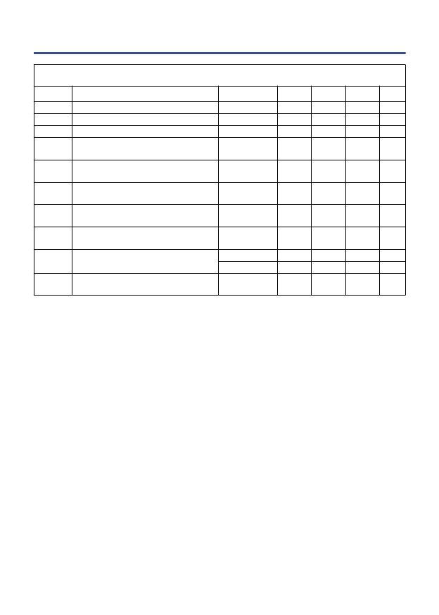
Table 12. ClockLock & ClockBoost Parameters for -2 Speed-Grade Devices
Symbol
Parameter
Condition
Min
Typ
Max
Unit
t
R
t
F
t
INDUTY
f
CLK1
Input rise time
Input fall time
Input duty cycle
Input clock frequency (ClockBoost clock
multiplication factor equals 1)
Input clock frequency (ClockBoost clock
multiplication factor equals 2)
Input deviation from user specification in
the software
(1)
t
INCLKSTB
Input clock stability (measured between
adjacent clocks)
t
LOCK
Time required for ClockLock or ClockBoost
to acquire lock
(3)
t
JITTER
Jitter on ClockLock or ClockBoost-
generated clock
(4)
5
5
ns
ns
%
MHz
40
25
60
80
f
CLK2
16
40
MHz
f
CLKDEV
25,000
PPM
100
ps
10
μ
s
t
INCLKSTB
< 100
t
INCLKSTB
< 50
250
(4)
200
(4)
60
ps
ps
%
t
OUTDUTY
Duty cycle for ClockLock or ClockBoost-
generated clock
40
50
相關(guān)PDF資料 |
PDF描述 |
|---|---|
| EP1K10 | Programmable Logic Device Family |
| EP1K100 | Programmable Logic Device Family |
| EP1K30 | Programmable Logic Device Family |
| EP1K50 | Programmable Logic Device Family |
| EP1S60B1508C5ES | Stratix Device Family Data Sheet |
相關(guān)代理商/技術(shù)參數(shù) |
參數(shù)描述 |
|---|---|
| EP1K30TI144-2N | 功能描述:FPGA - 現(xiàn)場(chǎng)可編程門(mén)陣列 FPGA - ACEX 1K 216 LABs 102 IOs RoHS:否 制造商:Altera Corporation 系列:Cyclone V E 柵極數(shù)量: 邏輯塊數(shù)量:943 內(nèi)嵌式塊RAM - EBR:1956 kbit 輸入/輸出端數(shù)量:128 最大工作頻率:800 MHz 工作電源電壓:1.1 V 最大工作溫度:+ 70 C 安裝風(fēng)格:SMD/SMT 封裝 / 箱體:FBGA-256 |
| EP1K50 | 制造商:未知廠家 制造商全稱(chēng):未知廠家 功能描述:Programmable Logic Device Family |
| EP1K50FC256-1 | 功能描述:FPGA - 現(xiàn)場(chǎng)可編程門(mén)陣列 FPGA - ACEX 1K 360 LABs 186 IOs RoHS:否 制造商:Altera Corporation 系列:Cyclone V E 柵極數(shù)量: 邏輯塊數(shù)量:943 內(nèi)嵌式塊RAM - EBR:1956 kbit 輸入/輸出端數(shù)量:128 最大工作頻率:800 MHz 工作電源電壓:1.1 V 最大工作溫度:+ 70 C 安裝風(fēng)格:SMD/SMT 封裝 / 箱體:FBGA-256 |
| EP1K50FC256-1DX | 制造商:未知廠家 制造商全稱(chēng):未知廠家 功能描述:Field Programmable Gate Array (FPGA) |
| EP1K50FC256-1F | 制造商:未知廠家 制造商全稱(chēng):未知廠家 功能描述:Field Programmable Gate Array (FPGA) |
發(fā)布緊急采購(gòu),3分鐘左右您將得到回復(fù)。