- 您現(xiàn)在的位置:買(mǎi)賣(mài)IC網(wǎng) > PDF目錄362742 > EP7211 (Cirrus Logic, Inc.) HIGH-PERFORMANCE ULTRA-LOW-POWER SYSTEM-ON-CHIP WITH LCD CONTROLLER PDF資料下載
參數(shù)資料
| 型號(hào): | EP7211 |
| 廠商: | Cirrus Logic, Inc. |
| 英文描述: | HIGH-PERFORMANCE ULTRA-LOW-POWER SYSTEM-ON-CHIP WITH LCD CONTROLLER |
| 中文描述: | 高性能超低功耗系統(tǒng)與LCD控制器芯片 |
| 文件頁(yè)數(shù): | 101/166頁(yè) |
| 文件大小: | 2623K |
| 代理商: | EP7211 |
第1頁(yè)第2頁(yè)第3頁(yè)第4頁(yè)第5頁(yè)第6頁(yè)第7頁(yè)第8頁(yè)第9頁(yè)第10頁(yè)第11頁(yè)第12頁(yè)第13頁(yè)第14頁(yè)第15頁(yè)第16頁(yè)第17頁(yè)第18頁(yè)第19頁(yè)第20頁(yè)第21頁(yè)第22頁(yè)第23頁(yè)第24頁(yè)第25頁(yè)第26頁(yè)第27頁(yè)第28頁(yè)第29頁(yè)第30頁(yè)第31頁(yè)第32頁(yè)第33頁(yè)第34頁(yè)第35頁(yè)第36頁(yè)第37頁(yè)第38頁(yè)第39頁(yè)第40頁(yè)第41頁(yè)第42頁(yè)第43頁(yè)第44頁(yè)第45頁(yè)第46頁(yè)第47頁(yè)第48頁(yè)第49頁(yè)第50頁(yè)第51頁(yè)第52頁(yè)第53頁(yè)第54頁(yè)第55頁(yè)第56頁(yè)第57頁(yè)第58頁(yè)第59頁(yè)第60頁(yè)第61頁(yè)第62頁(yè)第63頁(yè)第64頁(yè)第65頁(yè)第66頁(yè)第67頁(yè)第68頁(yè)第69頁(yè)第70頁(yè)第71頁(yè)第72頁(yè)第73頁(yè)第74頁(yè)第75頁(yè)第76頁(yè)第77頁(yè)第78頁(yè)第79頁(yè)第80頁(yè)第81頁(yè)第82頁(yè)第83頁(yè)第84頁(yè)第85頁(yè)第86頁(yè)第87頁(yè)第88頁(yè)第89頁(yè)第90頁(yè)第91頁(yè)第92頁(yè)第93頁(yè)第94頁(yè)第95頁(yè)第96頁(yè)第97頁(yè)第98頁(yè)第99頁(yè)第100頁(yè)當(dāng)前第101頁(yè)第102頁(yè)第103頁(yè)第104頁(yè)第105頁(yè)第106頁(yè)第107頁(yè)第108頁(yè)第109頁(yè)第110頁(yè)第111頁(yè)第112頁(yè)第113頁(yè)第114頁(yè)第115頁(yè)第116頁(yè)第117頁(yè)第118頁(yè)第119頁(yè)第120頁(yè)第121頁(yè)第122頁(yè)第123頁(yè)第124頁(yè)第125頁(yè)第126頁(yè)第127頁(yè)第128頁(yè)第129頁(yè)第130頁(yè)第131頁(yè)第132頁(yè)第133頁(yè)第134頁(yè)第135頁(yè)第136頁(yè)第137頁(yè)第138頁(yè)第139頁(yè)第140頁(yè)第141頁(yè)第142頁(yè)第143頁(yè)第144頁(yè)第145頁(yè)第146頁(yè)第147頁(yè)第148頁(yè)第149頁(yè)第150頁(yè)第151頁(yè)第152頁(yè)第153頁(yè)第154頁(yè)第155頁(yè)第156頁(yè)第157頁(yè)第158頁(yè)第159頁(yè)第160頁(yè)第161頁(yè)第162頁(yè)第163頁(yè)第164頁(yè)第165頁(yè)第166頁(yè)
EP7211
High-Performance Ultra-Low-Power System-on-Chip with LCD Controller
101
Register Descriptions
DS352PP3
JUL 2001
The previous table preserves compatibility with the previous devices, while allowing the previously
unused bit combinations to specify more variations of random and sequential wait states.
See the
AC Electrical Specification
section for more detail on bus timing.
The memory area decoded by CS6 is reserved for the on-chip SRAM, hence this does not require a
configuration field in MEMCFG2. It is automatically set up for 32-bit wide, no wait state accesses.
For the Boot ROM, it is automatically set up for 8-bit, no wait state accesses.
Chip selects
NCS4
and
NCS5
are used to select two CL-PS6700 PC CARD controller devices. These
have a multiplexed 16-bit wide address/data interface, and the configuration bytes in the MEMCFG2
register have no meaning when these interfaces are enabled.
5.4.3
DRFPR DRAM Refresh Period Register
ADDRESS: 0x8000.0200
The DRAM refresh period register is an 8-bit read/write register which enables refreshes and selects
the refresh period used by the DRAM controller for its periodic CAS before RAS refresh. The value
1
1
1
1
1
0
Bit
Description
6
SQAEN
: Sequential access enable. Setting this bit will enable sequential accesses that are on a quad
word boundary to take advantage of faster access times from devices that support page mode. The
sequential access will be faulted after four words, (to allow video refresh cycles to occur) even if the
access is part of a longer sequential access. In addition, when this bit is not set, non-sequential accesses
will have a single idle cycle inserted at least every four cycles so that the chip select is de-asserted period-
ically between accesses for easier debug.
7
CLKENB
: Expansion clock enable. Setting this bit enables the
EXPCLK
to be active during accesses to
the selected expansion device. This will provide a timing reference for devices that need to extend bus
cycles using the
EXPRDY
input. Back to back (but not necessarily page mode) accesses will result in a
continuous clock. This bit will only affect
EXPCLK
when the PLL is being used (i.e., in 73.728
–
18.432MHz
mode). When operating in 13 MHz mode, the
EXPCLK
pin is an input so cannot be affected by this regis-
ter bit. To save power internally, it should always be set to zero when operating in 13 MHz mode.
7
6:0
RFSHEN
RFDIV
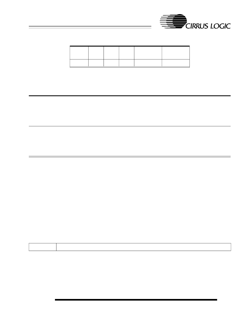
Table 5-6. Values of the Wait State Field at 36 MHz
(cont.)
Bit 3
Bit 2
Bit 1
Bit 0
Wait States
Random
Wait States
Sequential
相關(guān)PDF資料 |
PDF描述 |
|---|---|
| EP7211-CP-A | HIGH-PERFORMANCE ULTRA-LOW-POWER SYSTEM-ON-CHIP WITH LCD CONTROLLER |
| EP7211-CV-A | HIGH-PERFORMANCE ULTRA-LOW-POWER SYSTEM-ON-CHIP WITH LCD CONTROLLER |
| EP7212 | HIGH-PERFORMANCE, LOW-POWER SYSTEM-ON-CHIP WITH LCD CONTROLLER AND DIGITAL AUDIO INTERFACE(DAI) |
| EP7212-CB-A | HIGH-PERFORMANCE, LOW-POWER SYSTEM-ON-CHIP WITH LCD CONTROLLER AND DIGITAL AUDIO INTERFACE(DAI) |
| EP7212-CV-A | HIGH-PERFORMANCE, LOW-POWER SYSTEM-ON-CHIP WITH LCD CONTROLLER AND DIGITAL AUDIO INTERFACE(DAI) |
相關(guān)代理商/技術(shù)參數(shù) |
參數(shù)描述 |
|---|---|
| EP7211(208LQFP) | 制造商:未知廠家 制造商全稱:未知廠家 功能描述:Logic IC |
| EP7211(256PBGA) | 制造商:未知廠家 制造商全稱:未知廠家 功能描述:Logic IC |
| EP7211-CB-D | 制造商:Rochester Electronics LLC 功能描述:- Bulk |
| EP7211-CP-A | 制造商:CIRRUS 制造商全稱:Cirrus Logic 功能描述:HIGH-PERFORMANCE ULTRA-LOW-POWER SYSTEM-ON-CHIP WITH LCD CONTROLLER |
| EP7211-CV-A | 制造商:CIRRUS 制造商全稱:Cirrus Logic 功能描述:HIGH-PERFORMANCE ULTRA-LOW-POWER SYSTEM-ON-CHIP WITH LCD CONTROLLER |
發(fā)布緊急采購(gòu),3分鐘左右您將得到回復(fù)。