- 您現(xiàn)在的位置:買賣IC網(wǎng) > PDF目錄362799 > EV8802DJ-00A (Monolithic Power Systems, Inc.) Low Dropout 250mA Linear Regulator PDF資料下載
參數(shù)資料
| 型號(hào): | EV8802DJ-00A |
| 廠商: | Monolithic Power Systems, Inc. |
| 英文描述: | Low Dropout 250mA Linear Regulator |
| 中文描述: | 250mA的低壓差線性穩(wěn)壓器 |
| 文件頁數(shù): | 2/7頁 |
| 文件大小: | 283K |
| 代理商: | EV8802DJ-00A |
MP8802 – LOW DROPOUT, 250mA LINEAR REGULATOR
MP8802 Rev. 1.3
3/6/2006
www.MonolithicPower.com
2
MPS Proprietary Information. Unauthorized Photocopy and Duplication Prohibited.
2006 MPS. All Rights Reserved.
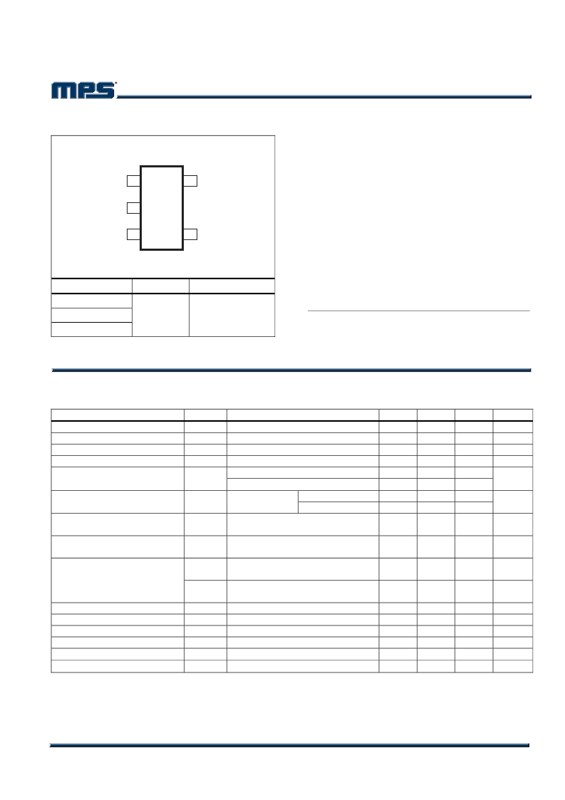
PACKAGE REFERENCE
Part Number**
MP8802DJ
–
2.5
MP8802DJ
–
2.85
MP8802DJ
–
3.3
Package
Temperature
TSOT23-5
–40
°
C to +85
°
C
**
For Tape & Reel, add suffix –Z (eg. MP8802DJ–2.85–Z)
For Lead Free, add suffix –LF (eg. MP8802DJ–2.85–LF–Z)
ABSOLUTE MAXIMUM RATINGS
(1)
IN Supply Voltage.......................–0.3V to +7.0V
FB Voltage.........................–0.3V to V
OUT
+ 0.3V
All Other Pins.................................–0.3V to +6V
Junction Temperature...............................150
°
C
Lead Temperature....................................260
°
C
Storage Temperature .............–65°C to +150
°
C
Recommended Operating Conditions
(2)
Input Voltage ..................................2.7V to 6.5V
Output Voltage.................................1.25V to 5V
Load Current...........................250mA Maximum
Operating Temperature .............–40
°
C to +85
°
C
Thermal Resistance
(3)
TSOT23-5..............................220.... 110..
°
C/W
θ
JA
θ
JC
Notes:
1) Exceeding these ratings may damage the device.
2) The device is not guaranteed to function outside of its
operating conditions.
3) Measured on approximately 1” square of 1 oz copper.
ELECTRICAL CHARACTERISTICS
V
IN
= 5V, T
A
= +25
°
C, unless otherwise noted.
Parameter
Operating Voltage
Output Voltage Accuracy
Ground Pin Current
Shutdown Current
Symbol Condition
I
OUT
= 1mA
I
OUT
= 1mA, V
OUT
= 1.25V to 5V
I
OUT
= 1mA–250mA
V
EN
= 0V, V
IN
= 5V
–40
°
C
≤
T
A
≤
+85
°
C
Min
2.7
2.0
1.197
1.194
Typ
(4)
±1.0
125
0.1
1.222
1.222
230
190
Max
6.5
2.0
155
1
1.246
1.249
Units
V
%
μA
μA
FB Regulation Voltage
V
V
OUT
= 3V
V
OUT
= 4V
Dropout Voltage
(5)
I
OUT
= 250mA
mV
Line Regulation
I
OUT
= 1mA,
V
IN
= (V
OUT
+ 0.5V) to 6.5V
(6)
I
OUT
= 1mA to 250mA,
V
IN
= V
OUT
+ 0.5V
(6)
V
IN
> V
OUT
+0.5V, C
OUT
= 2.2μF,
V
IN
(AC) = 100mV, f = 1kHz
V
IN
> V
OUT
+ 0.5V, C
OUT
= 2.2μF,
V
IN
(AC) = 100mV, f = 1MHz
f = 1kHz, C
FB
> 0.1μF, I
OUT
= 1mA
V
EN
= 0V, 5V
0.005
0.08
%/V
Load Regulation
0.001
0.02
%/mA
70
dB
PSRR
30
dB
Output Voltage Noise
EN Input High Voltage
EN Input Low Voltage
EN Input Bias Current
Thermal Protection
Thermal Protection Hysteresis
300
0.01
155
30
nV/
√
Hz
V
V
μA
°
C
°
C
1.5
1
0.4
Notes:
4) Parameter is guaranteed by design, not production tested.
5) Dropout Voltage is defined as the input to output differential when the output voltage drops 1% below its normal value.
6) V
IN
= 2.7V for V
OUT
= 1.25V to 2.2V
TOP VIEW
M
IN
GND
EN
1
2
3
5
4
OUT
FB
MP8802_PD01-TSOT23-5
相關(guān)PDF資料 |
PDF描述 |
|---|---|
| EVAL-AD1555 | Evaluation Board AD1555/1556 24-Bit ADC |
| EVAL-AD1556 | Evaluation Board AD1555/1556 24-Bit ADC |
| EVAL-AD1556EB | Evaluation Board AD1555/1556 24-Bit ADC |
| EVAL-AD1833AEB | 24-Bit, 192 kHz, DAC |
| EVAL-AD1833EB | Multichannel 24-Bit, 192 kHz, DAC |
相關(guān)代理商/技術(shù)參數(shù) |
參數(shù)描述 |
|---|---|
| EV8810 | 制造商:CMLMICRO 制造商全稱:CML Microcircuits 功能描述:The Product Data Amendment series of documents |
| EV-887408-VAL-01 | 制造商:AppliedMicro 功能描述:BLACKBIRD STORM VALIDATION KIT - Boxed Product (Development Kits) |
| EV8AQ160CTPY | 制造商:e2v technologies 功能描述:MULTI-CHANNEL 8-BIT ANALOGUE-TO-DIGITAL CONVERTER - Trays |
| EV8AQ160TPY-EB | 制造商:e2v technologies 功能描述:EVAL BOARD 8-BIT ADC - Trays |
| EV90 | 功能描述:消費(fèi)電池與相機(jī)電池 REORD 525-1209 GENERAL PURPOSE-6V RoHS:否 制造商:FDK Batteries 電池大小:CR1/3N 輸出電壓:3 V 容量:160 mAh 化學(xué)性質(zhì):Lithium 端接類型:Pressure Contacts 可再充電/不可再充電:Non-Rechargeable |
發(fā)布緊急采購,3分鐘左右您將得到回復(fù)。