- 您現(xiàn)在的位置:買賣IC網(wǎng) > PDF目錄362803 > EVAL-ADF4360-3EB1 (Analog Devices, Inc.) Integrated Synthesizer and VCO PDF資料下載
參數(shù)資料
| 型號(hào): | EVAL-ADF4360-3EB1 |
| 廠商: | Analog Devices, Inc. |
| 元件分類: | XO, clock |
| 英文描述: | Integrated Synthesizer and VCO |
| 中文描述: | 綜合合成器和VCO |
| 文件頁數(shù): | 9/24頁 |
| 文件大小: | 559K |
| 代理商: | EVAL-ADF4360-3EB1 |
ADF4360-3
CIRCUIT DESCRIPTION
REFERENCE INPUT SECTION
The reference input stage is shown in Figure 10. SW1 and SW2
are normally closed switches. SW3 is normally open. When
power-down is initiated, SW3 is closed, and SW1 and SW2 are
opened. This ensures that there is no loading of the REF
IN
pin
on power-down.
Rev. 0 | Page 9 of 24
0
BUFFER
TO R COUNTER
REF
IN
100k
NC
SW2
SW3
NO
NC
SW1
POWER-DOWN
CONTROL
Figure 10. Reference Input Stage
PRESCALER (P/P + 1)
The dual-modulus prescaler (P/P + 1), along with the A and B
counters, enables the large division ratio,
N
, to be realized (
N
=
BP
+
A
). The dual-modulus prescaler, operating at CML levels,
takes the clock from the VCO and divides it down to a manage-
able frequency for the CMOS A and B counters. The prescaler is
programmable. It can be set in software to 8/9, 16/17, or 32/33
and is based on a synchronous 4/5 core. There is a minimum
divide ratio possible for fully contiguous output frequencies;
this minimum is determined by P, the prescaler value, and is
given by (
P
2
P
).
A AND B COUNTERS
The A and B CMOS counters combine with the dual-modulus
prescaler to allow a wide range division ratio in the PLL feed-
back counter. The counters are specified to work when the pre-
scaler output is 300 MHz or less. Thus, with a VCO frequency of
2.5 GHz, a prescaler value of 16/17 is valid, but a value of 8/9 is
not valid.
Pulse Swallow Function
The A and B counters, in conjunction with the dual-modulus
prescaler, make it possible to generate output frequencies that
are spaced only by the reference frequency divided by
R
. The
VCO frequency equation is
(
)
R
f
A
B
P
f
REFIN
VCO
/
×
]
+
×
[
=
where:
f
VCO
is the output frequency of the VCO.
P
is the preset modulus of the dual-modulus prescaler (8/9,
16/17, and so on).
B
is the preset divide ratio of the binary 13-bit counter (3 to 8191).
A
is the preset divide ratio of the binary 5-bit swallow counter (0 to 31).
f
REFIN
is the external reference frequency oscillator.
N = BP + A
TO PFD
FROM VCO
N DIVIDER
MODULUS
CONTROL
LOAD
LOAD
13-BIT B
COUNTER
5-BIT A
COUNTER
PRESCALER
P/P+1
0
Figure 11. A and B Counters
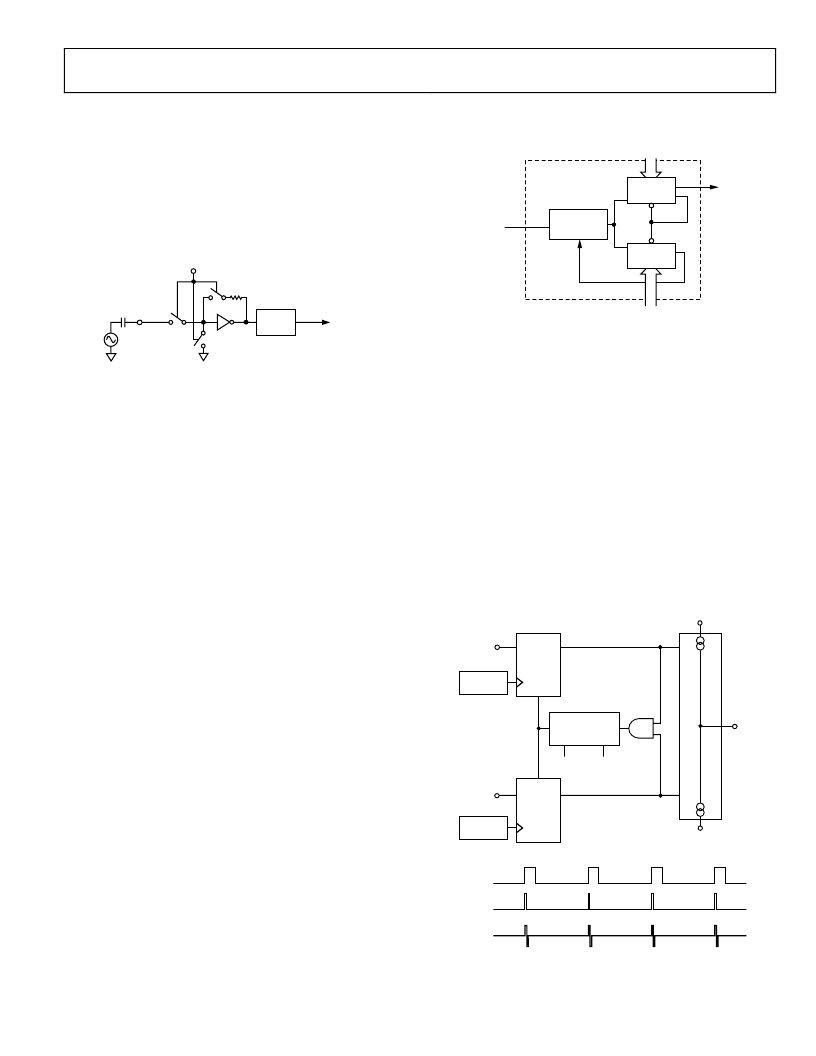
R COUNTER
The 14-bit R counter allows the input reference frequency to
be divided down to produce the reference clock to the phase
frequency detector (PFD). Division ratios from 1 to 16,383 are
allowed.
PFD AND CHARGE PUMP
The PFD takes inputs from the R counter and N counter (
N
=
BP
+
A
) and produces an output proportional to the phase and
frequency difference between them. Figure 12 is a simplified
schematic. The PFD includes a programmable delay element
that controls the width of the antibacklash pulse. This pulse
ensures that there is no dead zone in the PFD transfer function
and minimizes phase noise and reference spurs. Two bits in the
R counter latch, ABP2 and ABP1, control the width of the pulse
(see Table 9).
0
PROGRAMMABLE
DELAY
U3
CLR2
Q2
D2
U2
CLR1
Q1
D1
CHARGE
PUMP
DOWN
UP
HI
HI
U1
ABP1
ABP2
R DIVIDER
N DIVIDER
CP OUTPUT
R DIVIDER
N DIVIDER
CP
CPGND
V
P
Figure 12. PFD Simplified Schematic and Timing (In Lock)
相關(guān)PDF資料 |
PDF描述 |
|---|---|
| EVAL-ADF4360-5EB1 | Integrated Synthesizer and VCO |
| EVAL-ADF4360-6EB1 | Integrated Synthesizer and VCO |
| EVAL-ADF4360-8EB1 | Integrated Synthesizer and VCO |
| EVAL-ADF7012EB1 | Multichannel ISM Band FSK/GFSK/OOK/GOOK/ASK Transmitter |
| EVAL-ADF7012EB2 | Multichannel ISM Band FSK/GFSK/OOK/GOOK/ASK Transmitter |
相關(guān)代理商/技術(shù)參數(shù) |
參數(shù)描述 |
|---|---|
| EVAL-ADF4360-4EB1 | 制造商:AD 制造商全稱:Analog Devices 功能描述:Integrated Synthesizer and VCO |
| EVAL-ADF4360-4EBZ1 | 制造商:Analog Devices 功能描述:Evaluation Board Integrated Synthesizer And VCO 制造商:Analog Devices 功能描述:Evaluation Board I.C. |
| EVAL-ADF4360-5EB1 | 制造商:Analog Devices 功能描述:EVALUATION BOARD FOR ADF4360-5 |
| EVAL-ADF4360-5EBZ1 | 制造商:Analog Devices 功能描述: |
| EVAL-ADF4360-6EB1 | 制造商:AD 制造商全稱:Analog Devices 功能描述:Integrated Synthesizer and VCO |
發(fā)布緊急采購,3分鐘左右您將得到回復(fù)。