- 您現(xiàn)在的位置:買賣IC網(wǎng) > PDF目錄362803 > EVAL-ADN2819-CML (Analog Devices, Inc.) Multirate to 2.7 Gb/s Clock and Data Recovery IC with Integrated Limiting Amp PDF資料下載
參數(shù)資料
| 型號: | EVAL-ADN2819-CML |
| 廠商: | Analog Devices, Inc. |
| 元件分類: | 限幅放大器 |
| 英文描述: | Multirate to 2.7 Gb/s Clock and Data Recovery IC with Integrated Limiting Amp |
| 中文描述: | 多速率為2.7 Gb / s的集成時鐘和數(shù)據(jù)恢復芯片限幅放大器 |
| 文件頁數(shù): | 20/24頁 |
| 文件大小: | 570K |
| 代理商: | EVAL-ADN2819-CML |
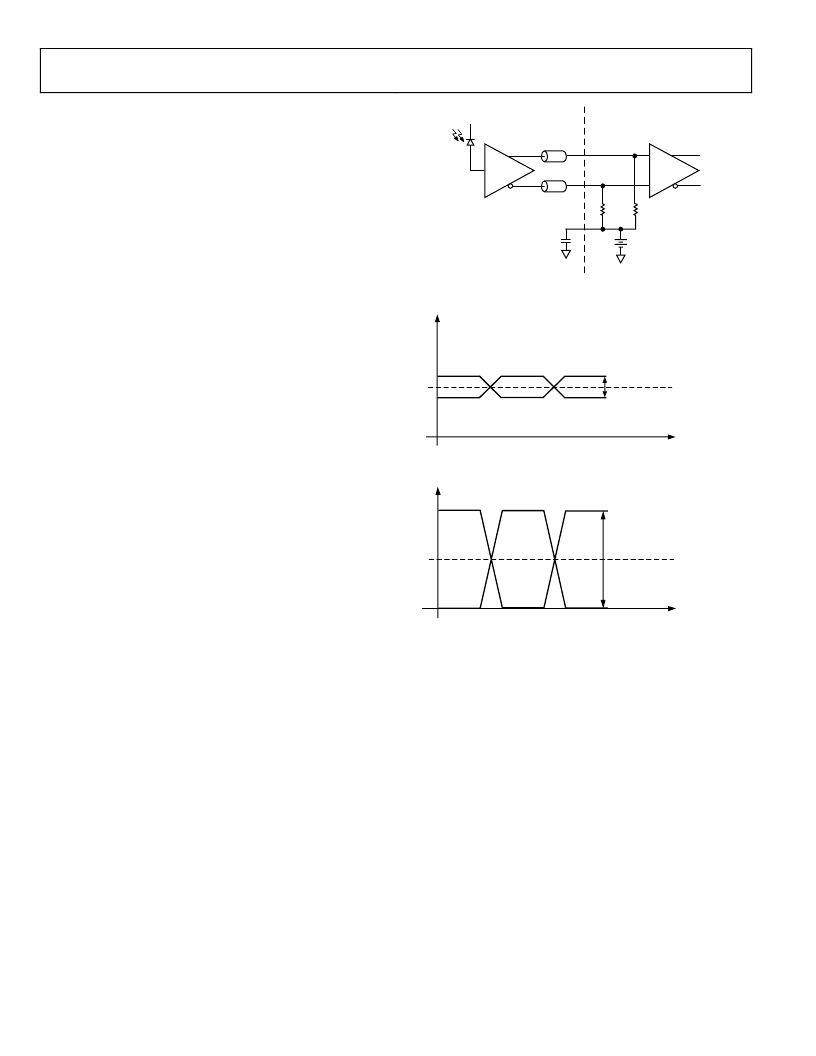
ADN2819
DC-COUPLED APPLICATION
The inputs to the ADN2819 can also be dc-coupled. This may
be necessary in burst mode applications where there are long
periods of CIDs and baseline wander cannot be tolerated. If the
inputs to the ADN2819 are dc-coupled, care must be taken not
to violate the input range and common-mode level
requirements of the ADN2819 (see Figure 26, Figure 27, and
Figure 28). If dc-coupling is required, and the output levels of
the TIA do not adhere to the levels shown in Figure 27 and
Figure 28, there needs to be level shifting and/or an attenuator
between the TIA outputs and the ADN2819 inputs.
Rev. B | Page 20 of 24
LOL TOGGLING DURING LOSS OF INPUT DATA
If the input data stream is lost due to a break in the optical link
(or for any reason), the clock output from the ADN2819 will
stay within 1000 ppm of the VCO center frequency as long as
there is a valid reference clock. The LOL pin toggles at a rate of
several kHz because the LOL pin toggles between a Logic 1 and
a Logic 0, while the frequency loop and phase loop swap control
of the VCO. The chain of events is as follows:
The ADN2819 is locked to the input data stream; LOL = 0.
The input data stream is lost due to a break in the link. The
VCO frequency drifts until the frequency error is greater
than 1000 ppm. LOL is asserted to a Logic 1 as control of
the VCO is passed back to the frequency loop.
The frequency loop pulls the VCO to within 500 ppm of its
center frequency. Control of the VCO is passed back to the
phase loop and LOL is deasserted to a Logic 0.
The phase loop tries to acquire, but there is no input data
present so the VCO frequency drifts.
The VCO frequency drifts until the frequency error is
greater than 1000 ppm. LOL is asserted to a Logic 1 as
control of the VCO is passed back to the frequency loop.
This process is repeated until a valid input data stream is
re-established.
50
50
ADN2819
0.1
μ
F
NIN
PIN
50
TIA
VREF
VCC
50
0
Figure 26. ADN2819 with DC-Coupled Inputs
V
CM
= 0.4V MIN
(DC-COUPLED)
V
SE
= 5mV MIN
PIN
NIN
V p-p = PIN – NIN = 2
×
V
SE
= 10mV AT SENSITIVITY
INPUT (V)
0
Figure 27. Minimum Allowed DC-Coupled Input Levels
INPUT (V)
PIN
NIN
V
CM
= 0.6V
(DC-COUPLED)
V
SE
= 1.2V MAX
V p-p = PIN – NIN = 2
×
V
SE
= 2.4V MAX
0
Figure 28. Maximum Allowed DC-Coupled Input Levels
相關(guān)PDF資料 |
PDF描述 |
|---|---|
| EVAL-ADN2843 | 10.709 Gbps Laser Diode Driver Chipset |
| EVAL-ADT7466EB | dBCool Remote Thermal Controller and Voltage Monitor |
| EVAL-ADUC846QS | MicroConverter, Dual 16-Bit ADCs with Embedded 62kB FLASH MCU |
| EVAL-ADUC846QSP | MicroConverter, Dual 16-Bit ADCs with Embedded 62kB FLASH MCU |
| EVAL-ADV7174EBM | Chip Scale PAL/NTSC Video Encoder with Advanced Power Management |
相關(guān)代理商/技術(shù)參數(shù) |
參數(shù)描述 |
|---|---|
| EVAL-ADN2830-U1 | 制造商:Analog Devices 功能描述:Avg power controller for CW lasers EVB 制造商:Analog Devices 功能描述:AVG POWER CONTROLLER FOR CW LASERS EVB - Bulk |
| EVAL-ADN2841-32-OP | 制造商:Analog Devices 功能描述:EVAL BD FOR OPTODRVRS, DUAL-LOOP 50MBPS-2.7GBPS LASER DIODE - Bulk |
| EVAL-ADN2841-48-OP | 制造商:Analog Devices 功能描述:Evaluation Board For Opto-Drivers, Dual-Loop 50Mbps-2.7Gbps LASER Diode Driver 制造商:Analog Devices 功能描述:EVAL BD FOR OPTODRVRS, DUAL-LOOP 50MBPS-2.7GBPS LASER DIODE - Bulk |
| EVAL-ADN2841-U2 | 制造商:Analog Devices 功能描述:EVAL BD FOR OPTODRVRS, DUAL-LOOP 50MBPS-2.7GBPS LASER DIODE - Bulk |
| EVAL-ADN2843 | 制造商:AD 制造商全稱:Analog Devices 功能描述:10.709 Gbps Laser Diode Driver Chipset |
發(fā)布緊急采購,3分鐘左右您將得到回復。