- 您現(xiàn)在的位置:買賣IC網(wǎng) > PDF目錄173420 > GE28F008B3BA70 (INTEL CORP) 1M X 8 FLASH 2.7V PROM, 70 ns, PBGA46 PDF資料下載
參數(shù)資料
| 型號(hào): | GE28F008B3BA70 |
| 廠商: | INTEL CORP |
| 元件分類: | PROM |
| 英文描述: | 1M X 8 FLASH 2.7V PROM, 70 ns, PBGA46 |
| 封裝: | VFBGA-46 |
| 文件頁(yè)數(shù): | 51/70頁(yè) |
| 文件大?。?/td> | 1215K |
| 代理商: | GE28F008B3BA70 |
第1頁(yè)第2頁(yè)第3頁(yè)第4頁(yè)第5頁(yè)第6頁(yè)第7頁(yè)第8頁(yè)第9頁(yè)第10頁(yè)第11頁(yè)第12頁(yè)第13頁(yè)第14頁(yè)第15頁(yè)第16頁(yè)第17頁(yè)第18頁(yè)第19頁(yè)第20頁(yè)第21頁(yè)第22頁(yè)第23頁(yè)第24頁(yè)第25頁(yè)第26頁(yè)第27頁(yè)第28頁(yè)第29頁(yè)第30頁(yè)第31頁(yè)第32頁(yè)第33頁(yè)第34頁(yè)第35頁(yè)第36頁(yè)第37頁(yè)第38頁(yè)第39頁(yè)第40頁(yè)第41頁(yè)第42頁(yè)第43頁(yè)第44頁(yè)第45頁(yè)第46頁(yè)第47頁(yè)第48頁(yè)第49頁(yè)第50頁(yè)當(dāng)前第51頁(yè)第52頁(yè)第53頁(yè)第54頁(yè)第55頁(yè)第56頁(yè)第57頁(yè)第58頁(yè)第59頁(yè)第60頁(yè)第61頁(yè)第62頁(yè)第63頁(yè)第64頁(yè)第65頁(yè)第66頁(yè)第67頁(yè)第68頁(yè)第69頁(yè)第70頁(yè)
28F008/800B3, 28F016/160B3, 28F320B3, 28F640B3
Datasheet
55
11.0
Modes of Operation
The flash memory has four read modes (read array, read identifier, read status, and read query; see
Figure 1, “B3 Architecture Block Diagram” on page 10), and two write modes (program and block
erase). Three additional modes (erase suspend to program, erase suspend to read, and program
suspend to read) are available only during suspended operations. Table 26, “Command Codes and
Descriptions” on page 55 summarizes the commands used to reach these modes. Appendix A,
“Write State Machine Current/Next States,” is a comprehensive chart showing the state transitions.
11.1
Read Array
When RP# transitions from VIL (reset) to VIH, the device defaults to read-array mode and will
respond to the read-control inputs (CE#, address inputs, and OE#) without any additional CUI
commands.
When the device is in read-array mode, four control signals control data output.
WE# must be logic high (VIH)
CE# must be logic low (VIL)
OE# must be logic low (VIL)
RP# must be logic high (VIH)
In addition, the address of the preferred location must be applied to the address pins. If the device is
not in read-array mode, as would be the case after a Program or Erase operation, the Read Array
command (FFH) must be written to the CUI before array reads can occur.
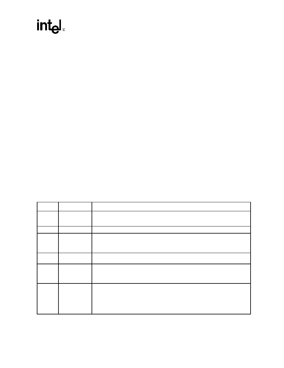
Table 26. Command Codes and Descriptions (Sheet 1 of 2)
Code
Device Mode
Description
00, 01,
60, 2F,
C0, 98
Invalid/
Reserved
Unassigned commands that must not be used. Intel reserves the right to redefine these codes
for future functions.
FF
Read Array
Places the device in read-array mode, such that array data will be output on the data pins.
40
Program Set-Up
This is a two-cycle command. The first cycle prepares the CUI for a program operation. The
second cycle latches addresses and data information and initiates the WSM to execute the
program algorithm. The flash outputs Status Register data when CE# or OE# is toggled. A
Read Array command is required after programming to read array data. See Section 11.4.
10
Alternate
Program Set-Up
(See 40H/Program Set-Up)
20
Erase Set-Up
Prepares the CUI for the Erase Confirm command. If the next command is not an Erase
Confirm command, then the CUI will (a) set both SR.4 and SR.5 of the Status Register to a “1,”
(b) place the device into the read-Status Register mode, and (c) wait for another command.
D0
Erase Confirm
Program / Erase
Resume
If the previous command was an Erase Set-Up command, then the CUI will close the address
and data latches, and begin erasing the block indicated on the address pins. During erase, the
device will only respond to the Read Status Register and Erase Suspend commands. The
device will output Status Register data when CE# or OE# is toggled.
If a Program or Erase operation was previously suspended, this command will resume that
operation.
相關(guān)PDF資料 |
PDF描述 |
|---|---|
| GE28F128W18BC60 | 8M X 16 FLASH 1.8V PROM, 60 ns, PBGA56 |
| GF-61-APC/90-L | BOARD TERMINATED, FEMALE, RF CONNECTOR, SOLDER |
| GF-61-APC/90L | BOARD TERMINATED, FEMALE, RF CONNECTOR, SOLDER, SOCKET |
| GF-61-APC-S | BOARD TERMINATED, FEMALE, RF CONNECTOR, SOLDER |
| GF-61-APC/S | BOARD TERMINATED, FEMALE, RF CONNECTOR, SOLDER |
相關(guān)代理商/技術(shù)參數(shù) |
參數(shù)描述 |
|---|---|
| GE28F008B3BA90 | 制造商:Intel 功能描述: |
| GE28F008B3TA90 | 制造商:INTEL 制造商全稱:Intel Corporation 功能描述:3 Volt Advanced Boot Block Flash Memory |
| GE28F128J3A-110 | 制造商:INTEL 制造商全稱:Intel Corporation 功能描述:Intel StrataFlash Memory (J3) |
| GE28F128J3A-115 | 制造商:INTEL 制造商全稱:Intel Corporation 功能描述:Intel StrataFlash Memory (J3) |
| GE28F128J3A-120 | 制造商:INTEL 制造商全稱:Intel Corporation 功能描述:Intel StrataFlash Memory (J3) |
發(fā)布緊急采購(gòu),3分鐘左右您將得到回復(fù)。