- 您現(xiàn)在的位置:買賣IC網(wǎng) > PDF目錄384399 > HE85750 (King Billion Electronics Co., Ltd.) 8-bit Micro-controller PDF資料下載
參數(shù)資料
| 型號: | HE85750 |
| 廠商: | King Billion Electronics Co., Ltd. |
| 英文描述: | 8-bit Micro-controller |
| 中文描述: | 8位微控制器 |
| 文件頁數(shù): | 2/23頁 |
| 文件大?。?/td> | 399K |
| 代理商: | HE85750 |
King Billion Electronics Co., Ltd
駿
億
電
子
股
份
有
限
公
司
HE85750
HE80000 SERIES
3.
Internal Block
2003/7/30
This specification is subject to change without notice. Please contact sales person for the latest version before use.
2
V1.52E
Please always keep in mind that ICE is different from IC. ICE is the whole set of HE80000 series IC, but
each IC is a subset of ICE. Never use any hardware resource that real IC didn't have, especially RAM and
register. KBIDS and compiler cannot prevent user to use some hardware resource that didn't exist. Please
check the following table and refer the abbreviation in HE80000 user's manual.
I.F.C. E.S.C. I.P.R PROM
DROM
TP
TP+1
◎
◎
◎
64KB
192KB
18-bit
◎
VO DAO OP PWM
LCD
COM*SEG
◎
—
◎
◎
2304~1152
32*64,48*48
1/7, 1/8
4.
Pin Description
RAM
2KB
PP
3-bit 8-bit 12~36
Rgr ChrgPmp
—
1,3/2,2,3
DP
I/O
DTMF WDT
—
LV2 LR LVG REC
◎
4:0
Timer
T1,T2,TB
S.R.
—
◎
Bias
◎
—
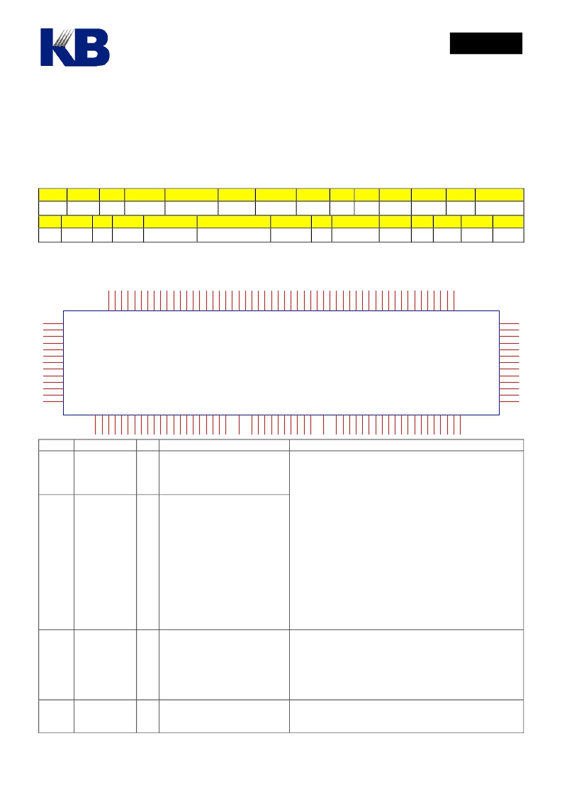
HE85750
1
2
3
4
5
6
7
8
9
1
1
1
1
1
1
1
1
1
1
2
2
2
2
2
2
2
2
2
2
3
3
3
3
3
3
3
3
3
3
4
4
4
4
4
4
4
4
4
4
5
5
5
5
54
55
56
57
58
59
60
61
62
63
64
65
66
6
6
6
7
7
7
7
7
7
7
7
7
7
8
8
8
8
8
8
8
8
8
8
9
9
9
9
9
9
9
9
9
9
1
1
1
1
1
1
1
1
1
1
1
1
1
1
1
1
1
1
1
1
1
121
122
123
124
125
126
127
128
129
130
131
132
133
L
L
L
L
L
L
L
L
L
L
L
G
V
O
O
O
R
F
F
T
S
S
V
P
P
P
P
P
P
P
P
G
P
P
P
P
P
C
C
C
C
C
C
C
C
C
C
C
C
C
C
C
C
CMSG32
CMSG33
CMSG34
CMSG35
CMSG36
CMSG37
CMSG38
CMSG39
CMSG40
CMSG41
CMSG42
CMSG43
CMSG44
C
C
C
S
S
S
S
S
S
S
S
S
S
S
S
S
S
S
S
S
S
S
S
S
S
S
S
P
P
P
P
P
P
P
P
P
P
P
P
P
P
P
P
P
P
P
P
P
P
P
P
C
C
C
COM12
COM11
COM10
COM9
COM8
COM7
COM6
COM5
COM4
COM3
COM2
COM1
COM0
Pin No
Pin Name
I/O
Function
fast
Description
19,
18
FXI,
FXO
B,
O
External
Connecting to crystal or RC to
generate 32.768 kHz ~ 8MHz
frequency.
clock
pin.
22,
21
SXI,
SXO
I,
O
External
Connecting with 32768
crystal or resistor as slow clock
and providing clock source for
LCD
display,
Time-Base and other internal
blocks.
slow
clock
pin.
Hz
TIMER1,
Mask option setting
:
MO_FCK/SCKN= 00
:
Slow Clock only
01
:
Illegal
10
:
Dual Clock
11
:
Fast Clock only
MO_FOSCE = 0
:
Internal fast osc.
= 1
:
External fast osc.
MO_FXTAL = 0
:
RC osc. for fast clock
= 1
:
X’tal osc. for fast clock
MO_SXTAL = 0
:
RC for 32768 Hz clock
= 1
:
X’tal for 32768 Hz clock
Use OP1 and OP2 to switch among different operation mode
(NORMAL, SLOW, IDEL and SLEEP). In Dual Clock
mode, the main system clock is still the Fast Clock. The
32768 Hz clock is for LCD and Timer 1 only.
Level trigger, active low. Except for using this pin, using
mask option (MO_PORE=1) could enable IC build-in
Power-on reset circuit.
Besides, MO_WDTE can set Watch Dog Timer
:
MO_WDTE=0
:
Disable Watch Dog Timer
=1
:
Enable Watch Dog Timer
Please bond this pin and add a test point on PCB for
debugging. Please connect this pin with zero ohm resistor
to GND.
17
RSTP_N
I
System Reset.
20
TSTP_P
I
Test Pin
相關(guān)PDF資料 |
PDF描述 |
|---|---|
| HE89410 | 8-BIT MICRO-CONTROLLER |
| HE89810 | 8-BIT MICRO-CONTROLLER |
| HE89820 | 8-BIT MICRO-CONTROLLER |
| HE89A20 | 8-BIT MICRO-CONTROLLER |
| HE89A21 | 8-BIT MICRO-CONTROLLER |
相關(guān)代理商/技術(shù)參數(shù) |
參數(shù)描述 |
|---|---|
| HE85750(S) | 制造商:未知廠家 制造商全稱:未知廠家 功能描述: |
| HE861 | 制造商:BOWEI 制造商全稱:BOWEI 功能描述:Broadband Amplifier |
| HE863AUD102T007 | 制造商:Telit 功能描述: |
| HE863EUD102T016 | 制造商:Telit 功能描述: |
| HE863EUR102T007 | 制造商:Telit 功能描述: |
發(fā)布緊急采購,3分鐘左右您將得到回復(fù)。