- 您現(xiàn)在的位置:買賣IC網(wǎng) > PDF目錄384402 > HF88M08 (King Billion Electronics Co., Ltd.) 512K x 8 bit Mask ROM PDF資料下載
參數(shù)資料
| 型號: | HF88M08 |
| 廠商: | King Billion Electronics Co., Ltd. |
| 英文描述: | 512K x 8 bit Mask ROM |
| 中文描述: | 為512k × 8位掩模ROM |
| 文件頁數(shù): | 4/19頁 |
| 文件大?。?/td> | 320K |
| 代理商: | HF88M08 |
King Billion Electronics Co., Ltd
駿 億 電 子 股 份 有 限 公 司
HF88M08
January 16, 2004
This specification is subject to change without notice. Please contact sales person for the latest version before use.
Page 4 of 19
V1.11
4
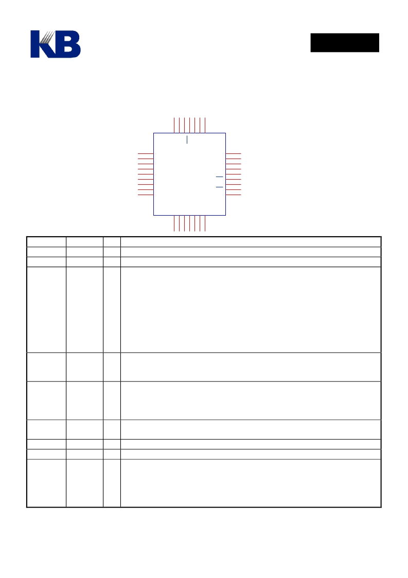
Pin Description
HF88M08-PLCC32
11
12
2
9
8
7
6
5
4
29
28
27
26
24
23
22
3
3
3
2
25
13
1
1
1
1
2
21
3
1
1
1
P01
P00
P02
P03
P04
P05
P06
P07
P
P16
P15
P10
P11
OE
P12
CE
P
R
R
R
P13
D0
D
D
D
D
D
D7
V
V
W
D
Symbol
VDD
VSS
CEn
Pin No. I/O
32
16
22
Description
P Positive power supply input pin.
P Gound pin.
I
The CEn (Chip Enable) input is the device selection and power control for
internal Mask ROM array. Whenever CEn goes high, the internal Mask
ROM will enter standby (power saving) mode and accesses to internal
registers are inhibited. Otherwise, it is in active mode and the contents of
the ROM and registers can be accessed. Please note that only accesses to
the internal registers are inhibited, but the status of I/O registers are not
affected by the CEn pin and will remain unchanged. CEn is also useful to
uniquely select a certain device for applications where multiple-chip array is
required.
I
WEn controls writing to internal registers such as the Output Port Registers,
Direction Registers, Address Counter and Data on D7 ~ D0 are latched on
the rising edge of the WE pulse.
I
OEn (Output Enable) is the output control which gates ROM array data,
expansion I/O ports, Direction Registers to the data I/O pins D7 ~ D0. The
internal Address Counter will automatically increment by one with each
rising edge of OEn pin in Sequentially Read mode.
I
Register Select pins RS2 ~ RS0 for accessing ROM data, Address Counter,
as well as expansion I/O ports.
I/O Bi-directional I/O port P1.
I/O Bi-directional I/O port P0.
IO The Bi-directional Data I/O pins are used to input Starting Address, setting
the Expansion I/O direction and Output Registers, and to output ROM array
data during read operations, contents of I/O Registers and status of input
pins. The D7 ~ D7 float to high-impedance when the chip is deselected (CEn
high) or when the outputs are disabled.
WEn
1
OEn
24
RS2~RS0
P17 ~ P10
P07 ~ P00
D7 ~ D0
21 ~ 17,
15 ~13
相關(guān)PDF資料 |
PDF描述 |
|---|---|
| HF88M32B | command interfaced 4M x 8 bit Mask ROM |
| HF88S05 | command mode SRAM device |
| HFA1105 | 144 MACROCELL 5 VOLT ISP CPLD - NOT RECOMMENDED for NEW DESIGN |
| HFA1105IP | 330MHz, Low Power, Current Feedback Video Operational Amplifier |
| HFA1105IB | Circular Connector; MIL SPEC:MIL-C-26482, Series I, Solder; Body Material:Aluminum; Series:PT06; No. of Contacts:41; Connector Shell Size:22; Connecting Termination:Solder; Circular Shell Style:Straight Plug; Body Style:Straight |
相關(guān)代理商/技術(shù)參數(shù) |
參數(shù)描述 |
|---|---|
| HF88M08(S) | 制造商:未知廠家 制造商全稱:未知廠家 功能描述: |
| HF88M32(S) | 制造商:未知廠家 制造商全稱:未知廠家 功能描述: |
| HF88M32B | 制造商:KB 制造商全稱:KB 功能描述:command interfaced 4M x 8 bit Mask ROM |
| HF88M32B(S) | 制造商:未知廠家 制造商全稱:未知廠家 功能描述: |
| HF88S05 | 制造商:KB 制造商全稱:KB 功能描述:command mode SRAM device |
發(fā)布緊急采購,3分鐘左右您將得到回復(fù)。