- 您現(xiàn)在的位置:買(mǎi)賣(mài)IC網(wǎng) > PDF目錄384403 > HFA3841 (Intersil Corporation) 288 MACROCELL 3.3 VOLT ISP CPLD PDF資料下載
參數(shù)資料
| 型號(hào): | HFA3841 |
| 廠商: | Intersil Corporation |
| 英文描述: | 288 MACROCELL 3.3 VOLT ISP CPLD |
| 中文描述: | 無(wú)線局域網(wǎng)媒體訪問(wèn)控制器 |
| 文件頁(yè)數(shù): | 20/27頁(yè) |
| 文件大小: | 211K |
| 代理商: | HFA3841 |
第1頁(yè)第2頁(yè)第3頁(yè)第4頁(yè)第5頁(yè)第6頁(yè)第7頁(yè)第8頁(yè)第9頁(yè)第10頁(yè)第11頁(yè)第12頁(yè)第13頁(yè)第14頁(yè)第15頁(yè)第16頁(yè)第17頁(yè)第18頁(yè)第19頁(yè)當(dāng)前第20頁(yè)第21頁(yè)第22頁(yè)第23頁(yè)第24頁(yè)第25頁(yè)第26頁(yè)第27頁(yè)
20
PHY Interface
The HFA3841 is intended to support the PRISM family of
Baseband processors with no additional components. This
family currently includes the HFA3860B and HFA3861 DSSS
baseband processors and the other ICs in the PRISM WLAN
chip set. (Other baseband processors may be supported
with custom firmware. See your sales representative for
more information). The HFA3841 interfaces to the HFA386X
baseband processors through two serial interfaces. The
Modem Management Interface (MMI) is used to read and
write internal registers in the baseband processor and
access per-packet PLCP information. The Modem Data
Interface (MDI) provides the receive and transmit data paths
which transfer the actual MPDU data.
Serial Control Port (MMI)
The HFA3841 has a serial port that is used to program the
baseband processor. There are individual chip selects and
shared clock and data lines.
The MMI is used to program the registers and functionality of
the PHY baseband processor.
PHY BASEBAND PROCESSOR
The PHY baseband processor is programmed by HFA3841
firmware.
The PRISM II baseband processor mode works as follows:
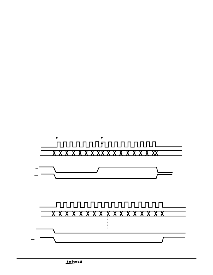
The Control Port consists of 4 signals: SD (serial data),
SCLK (serial clock), R/W (read/write) and CS_BAR (active-
low chip select).
Control Port signaling for read and write operations is
illustrated in Figures 16 and 17 respectively. Detailed timing
relationships appear in Figure 18 and timing specifications
are contained in Table 1.
The BBP always uses the rising edge when clocking data on
the Control Port. This means that when the BBP is receiving
data it uses the rising edge of clock to sample; when driving
data, transitions occur on the rising edge.
Address bits 6 through 1 are significant for selecting
configuration registers. Address bits 7 and 0 are unused.
See the BBP Programming section for register addresses
and suggested values.
For read operations, the rising edge of R/W must occur after
the 7th but prior to the 8th rising edge of SCLK. This ensures
that the first data bit is clocked out of the BBP prior to the
edge used to clock it into the MAC.
For more detailed information on the Control Port and BBP
register programming see the HFA386x data sheets.
7
6
5
4
3
2
1
0
7
6
5
4
3
2
1
0
7
6
5
4
3
2
1
0
7
6 5
4
3
2
7
6
1
0
SCLK
FIRST DATABIT OUT
MSB
ADDRESS IN
DATA OUT
MSB
LSB
FIRST ADDRESS BIT
SD
R/W
CS
FIGURE 16. PRISM II BASEBAND PROCESSOR CONTROL PORT READ TIMING
7
6
5
4
3
2
1
0
7
6
5
4
3
2
1
0
7
6
5
4
3
2
1
0
7
6
5
4
3
2
1
0
SCLK
MSB
ADDRESS IN
MSB
DATA IN
LSB
SD
R/W
CS
FIGURE 17. PRISM II BASEBAND PROCESSOR SERIAL CONTROL PORT WRITE TIMING
Preliminary - HFA3841
相關(guān)PDF資料 |
PDF描述 |
|---|---|
| HFA3841CN | 288 MACROCELL 3.3 VOLT ISP CPLD |
| HFA3841CN96 | Wireless LAN Medium Access Controller |
| HFA3842A | PCMCIA/USB Wireless LAN Medium Access Controller |
| HFA3842AIN | 3.3V 288-mc CPLD |
| HFA3842AIN-TK | Circular Connector; No. of Contacts:41; Series:MS27473; Body Material:Aluminum; Connecting Termination:Crimp; Connector Shell Size:20; Circular Contact Gender:Socket; Circular Shell Style:Straight Plug; Insert Arrangement:20-41 RoHS Compliant: No |
相關(guān)代理商/技術(shù)參數(shù) |
參數(shù)描述 |
|---|---|
| HFA3841CN | 制造商:Rochester Electronics LLC 功能描述:- Bulk |
| HFA3841CN96 | 制造商:INTERSIL 制造商全稱:Intersil Corporation 功能描述:Wireless LAN Medium Access Controller |
| HFA3842 | 制造商:INTERSIL 制造商全稱:Intersil Corporation 功能描述:Wireless LAN Medium Access Controller |
| HFA3842A | 制造商:INTERSIL 制造商全稱:Intersil Corporation 功能描述:PCMCIA/USB Wireless LAN Medium Access Controller |
| HFA3842AIN | 制造商:INTERSIL 制造商全稱:Intersil Corporation 功能描述:PCMCIA/USB Wireless LAN Medium Access Controller |
發(fā)布緊急采購(gòu),3分鐘左右您將得到回復(fù)。