- 您現(xiàn)在的位置:買賣IC網(wǎng) > PDF目錄384405 > HGT1S7N60C3D (FAIRCHILD SEMICONDUCTOR CORP) 14A, 600V, UFS Series N-Channel IGBT with Anti-Parallel Hyperfast Diodes PDF資料下載
參數(shù)資料
| 型號(hào): | HGT1S7N60C3D |
| 廠商: | FAIRCHILD SEMICONDUCTOR CORP |
| 元件分類: | 功率晶體管 |
| 英文描述: | 14A, 600V, UFS Series N-Channel IGBT with Anti-Parallel Hyperfast Diodes |
| 中文描述: | 14 A, 600 V, N-CHANNEL IGBT, TO-262AA |
| 封裝: | TO-262, 3PIN |
| 文件頁數(shù): | 1/7頁 |
| 文件大?。?/td> | 197K |
| 代理商: | HGT1S7N60C3D |
S E M I C O N D U C T O R
3-22
HGTP7N60C3D, HGT1S7N60C3D,
HGT1S7N60C3DS
14A, 600V, UFS Series N-Channel IGBT
with Anti-Parallel Hyperfast Diodes
Features
14A, 600V at T
C
= 25
o
C
600V Switching SOA Capability
Typical Fall Time . . . . . . . . . . . . . . 140ns at T
J
= 150
o
C
Short Circuit Rating
Low Conduction Loss
Hyperfast Anti-Parallel Diode
Description
The HGTP7N60C3D, HGT1S7N60C3D and HGT1S7N60C3DS
are MOS gated high voltage switching devices combining the
best features of MOSFETs and bipolar transistors. These
devices have the high input impedance of a MOSFET and the
low on-state conduction loss of a bipolar transistor. The much
lower on-state voltage drop varies only moderately between
25
o
C and 150
o
C. The IGBT used is developmental type
TA49115. The diode used in anti-parallel with the IGBT is devel-
opmental type TA49057.
The IGBT is ideal for many high voltage switching applications
operating at moderate frequencies where low conduction losses
are essential, such as: AC and DC motor controls, power sup-
plies and drivers for solenoids, relays and contactors
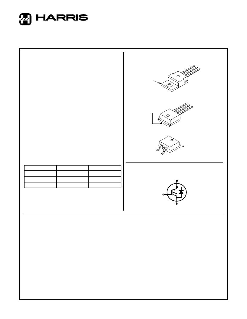
Packaging
JEDEC TO-220AB
JEDEC TO-262AA
JEDEC TO-263AB
Terminal Diagram
N-CHANNEL ENHANCEMENT MODE
Absolute Maximum Ratings
T
C
= 25
o
C, Unless Otherwise Specified
PACKAGING AVAILABILITY
PART NUMBER
PACKAGE
BRAND
HGTP7N60C3D
TO-220AB
G7N60C3D
HGT1S7N60C3D
TO-262AA
G7N60C3D
HGT1S7N60C3DS
TO-263AB
G7N60C3D
NOTE: When ordering, use the entire part number. Add the suffix 9A to
obtain the TO-263AB variant in tape and reel, i.e. HGT1S7N60C3DS9A.
Formerly Developmental Type TA49121.
GATE
COLLECTOR (FLANGE)
EMITTER
COLLECTOR
A
EMITTER
COLLECTOR
GATE
COLLECTOR
(FLANGE)
A
A
M
COLLECTOR
(FLANGE)
GATE
EMITTER
C
E
G
HGTP7N60C3D, HGT1S7N60C3D
HGT1S7N60C3DS
600
UNITS
V
Collector-Emitter Voltage . . . . . . . . . . . . . . . . . . . . . . . . . . . . . . . . . . . . . . . . . . . .BV
CES
Collector Current Continuous
At T
C
= 25
o
C. . . . . . . . . . . . . . . . . . . . . . . . . . . . . . . . . . . . . . . . . . . . . . . . . . . . . .I
C25
At T
C
= 110
o
C. . . . . . . . . . . . . . . . . . . . . . . . . . . . . . . . . . . . . . . . . . . . . . . . . . . . I
C110
Average Diode Forward Current at 110
o
C . . . . . . . . . . . . . . . . . . . . . . . . . . . . . . . I
(AVG)
Collector Current Pulsed (Note 1). . . . . . . . . . . . . . . . . . . . . . . . . . . . . . . . . . . . . . . . I
CM
Gate-Emitter Voltage Continuous . . . . . . . . . . . . . . . . . . . . . . . . . . . . . . . . . . . . . . .V
GES
Gate-Emitter Voltage Pulsed. . . . . . . . . . . . . . . . . . . . . . . . . . . . . . . . . . . . . . . . . . V
GEM
Switching Safe Operating Area at T
J
= 150
o
C, Figure 14 . . . . . . . . . . . . . . . . . . . SSOA
Power Dissipation Total at T
C
= 25
o
C . . . . . . . . . . . . . . . . . . . . . . . . . . . . . . . . . . . . . P
D
Power Dissipation Derating T
C
> 25
o
C. . . . . . . . . . . . . . . . . . . . . . . . . . . . . . . . . . . . . . .
Operating and Storage Junction Temperature Range . . . . . . . . . . . . . . . . . . . . T
J
, T
STG
Maximum Lead Temperature for Soldering. . . . . . . . . . . . . . . . . . . . . . . . . . . . . . . . . . T
L
Short Circuit Withstand Time (Note 2) at V
GE
= 15V . . . . . . . . . . . . . . . . . . . . . . . . . .t
SC
Short Circuit Withstand Time (Note 2) at V
GE
= 10V . . . . . . . . . . . . . . . . . . . . . . . . . .t
SC
NOTE:
1. Repetitive Rating: Pulse width limited by maximum junction temperature.
2. V
CE(PK)
= 360V, T
J
= 125
o
C, R
GE
= 50
.
14
7
8
56
±
20
±
30
A
A
A
A
V
V
40A at 480V
60
0.487
-40 to 150
260
1
8
W
W/
o
C
o
C
o
C
μ
s
μ
s
January 1997
CAUTION: These devices are sensitive to electrostatic discharge. Users should follow proper ESD Handling Procedures.
Copyright
Harris Corporation 1997
File Number
4150.1
相關(guān)PDF資料 |
PDF描述 |
|---|---|
| HGTP7N60C3D | 72 MACROCELL 3.3 VOLT ISP CPLD |
| HGTP7N60C3D | 3.3V 72-mc CPLD |
| HGT1S7N60C3DS | 14A, 600V, UFS Series N-Channel IGBT with Anti-Parallel Hyperfast Diodes |
| HGT4E20N60A4DS | CONNECTOR ACCESSORY |
| HGT4E30N60B3DS | CONNECTOR ACCESSORY |
相關(guān)代理商/技術(shù)參數(shù) |
參數(shù)描述 |
|---|---|
| HGT1S7N60C3DS | 功能描述:IGBT 晶體管 7A 600V TF=275NS RoHS:否 制造商:Fairchild Semiconductor 配置: 集電極—發(fā)射極最大電壓 VCEO:650 V 集電極—射極飽和電壓:2.3 V 柵極/發(fā)射極最大電壓:20 V 在25 C的連續(xù)集電極電流:150 A 柵極—射極漏泄電流:400 nA 功率耗散:187 W 最大工作溫度: 封裝 / 箱體:TO-247 封裝:Tube |
| HGT1S7N60C3DS9A | 功能描述:IGBT 晶體管 14a 600V N-Ch IGBT UFS Series RoHS:否 制造商:Fairchild Semiconductor 配置: 集電極—發(fā)射極最大電壓 VCEO:650 V 集電極—射極飽和電壓:2.3 V 柵極/發(fā)射極最大電壓:20 V 在25 C的連續(xù)集電極電流:150 A 柵極—射極漏泄電流:400 nA 功率耗散:187 W 最大工作溫度: 封裝 / 箱體:TO-247 封裝:Tube |
| HGT1Y40N60B3D | 制造商:FAIRCHILD 制造商全稱:Fairchild Semiconductor 功能描述:70A, 600V, UFS Series N-Channel IGBT with Anti-Parallel Hyperfast Diodes |
| HGT1Y40N60C3D | 制造商:未知廠家 制造商全稱:未知廠家 功能描述:TRANSISTOR | IGBT | N-CHAN | 600V V(BR)CES | 40A I(C) | TO-264 |
| HGT4E20N60A4DS | 功能描述:IGBT 晶體管 TO-268 RoHS:否 制造商:Fairchild Semiconductor 配置: 集電極—發(fā)射極最大電壓 VCEO:650 V 集電極—射極飽和電壓:2.3 V 柵極/發(fā)射極最大電壓:20 V 在25 C的連續(xù)集電極電流:150 A 柵極—射極漏泄電流:400 nA 功率耗散:187 W 最大工作溫度: 封裝 / 箱體:TO-247 封裝:Tube |
發(fā)布緊急采購,3分鐘左右您將得到回復(fù)。