- 您現(xiàn)在的位置:買賣IC網(wǎng) > PDF目錄384413 > HI-3584PQI-10 (HOLT INTEGRATED CIRCUITS INC) Enhanced ARINC 429 3.3V Serial Transmitter and Dual Receiver PDF資料下載
參數(shù)資料
| 型號(hào): | HI-3584PQI-10 |
| 廠商: | HOLT INTEGRATED CIRCUITS INC |
| 元件分類: | 微控制器/微處理器 |
| 英文描述: | Enhanced ARINC 429 3.3V Serial Transmitter and Dual Receiver |
| 中文描述: | 1 CHANNEL(S), 125K bps, SERIAL COMM CONTROLLER, PQFP52 |
| 封裝: | PLASTIC, QFP-52 |
| 文件頁(yè)數(shù): | 3/15頁(yè) |
| 文件大?。?/td> | 327K |
| 代理商: | HI-3584PQI-10 |
第1頁(yè)第2頁(yè)當(dāng)前第3頁(yè)第4頁(yè)第5頁(yè)第6頁(yè)第7頁(yè)第8頁(yè)第9頁(yè)第10頁(yè)第11頁(yè)第12頁(yè)第13頁(yè)第14頁(yè)第15頁(yè)
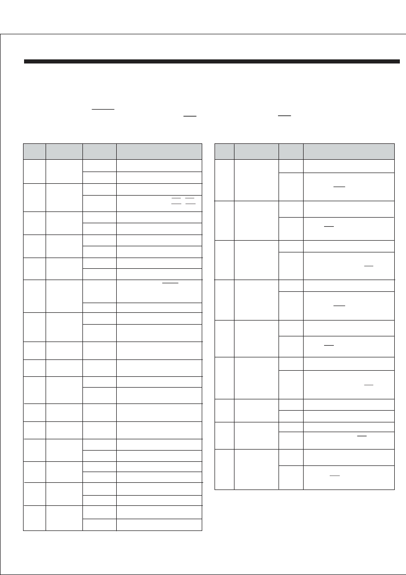
SR
Bit
FUNCTION
STATE
DESCRIPTION
SR0
Data ready
(Receiver 1)
0
Receiver 1 FIFO empty
1
Receiver 1 FIFO contains valid data
Resets to zero when all data has
been read.
pin is the inverse of
this bit
SR1
FIFO half full
(Receiver 1)
0
Receiver 1 FIFO holds less than 16
words
1
Receiver 1 FIFO holds at least 16
words.
pin is the inverse of
this bit.
SR2
FIFO full
(Receiver 1)
0
Receiver 1 FIFO not full
1
Receiver 1 FIFO full. To avoid data
loss, the FIFO must be read within
one ARINC word period.
the inverse of this bit
pin is
SR3
Data ready
(Receiver 2)
0
Receiver 2 FIFO empty
1
Receiver 2 FIFO contains valid data
Resets to zero when all data has
been read.
pin is the inverse of
this bit
SR4
FIFO half full
(Receiver 2)
0
Receiver 2 FIFO holds less than 16
words
1
Receiver 2 FIFO holds at least 16
words.
pin is the inverse of
this bit.
SR5
FIFO full
(Receiver 2)
0
Receiver 2 FIFO not full
1
Receiver 2 FIFO full. To avoid data
loss, the FIFO must be read within
one ARINC word period.
the inverse of this bit
pin is
SR6
Transmitter FIFO
empty
0
Transmitter FIFO not empty
1
Transmitter FIFO empty.
SR7
Transmitter FIFO
full
0
Transmitter FIFO not full
1
Transmitter FIFO full.
inverse of this bit.
pin is the
SR8
Transmitter FIFO
half full
0
Transmitter FIFO contains less than
16 words
1
Transmitter FIFO contains at least
16 words.
pin is the
inverse of this bit.
D/R1
HF1
FF1
D/R2
HF2
FF2
FFT
HFT
FUNCTIONAL DESCRIPTION
CONTROL WORD REGISTER
The HI-3584 contains a 16-bit control register which is used to con-
figure the device. The control register bits CR0 - CR15 are loaded
from BD00 - BD15 when
ter contents are output on the databus when SEL = 1 and
pulsed low. Each bit of the control register has the following func-
tion:
is pulsed low. The control regis-
is
CWSTR
RSR
STATUS REGISTER
The HI-3584 contains a 9-bit status register which can be interro-
gated to determine the status of the ARINC receivers, data FIFOs
and transmitter. The contents of the status register are output on
BD00 - BD08 when the
pin is taken low and SEL = 0. Unused
bits are output as zeros. The following table defines the status reg-
ister bits.
RSR
HOLT INTEGRATED CIRCUITS
3
HI-3584
CR
Bit
FUNCTION
STATE
DESCRIPTION
CR0
Receiver 1
Data clock
0
Data rate = CLK/10
Select
1
Data rate = CLK/80
CR1
Label Memory
Read / Write
0
Normal operation
1
Load 16 labels using
Read 16 labels using
/
/
CR2
Enable Label
Recognition
(Receiver 1)
0
Disable label recognition
1
Enable label recognition
CR3
Enable Label
Recognition
(Receiver 2)
0
Disable Label Recognition
1
Enable Label recognition
CR4
Enable
32nd bit
as parity
0
Transmitter 32nd bit is data
1
Transmitter 32nd bit is parity
CR5
Self Test
0
The 429DO and
outputs are internally connected
to the receiver logic inputs
digital
1
Normal operation
CR6
Receiver 1
decoder
0
Receiver 1 decoder disabled
1
ARINC bits 9 and 10 must match
CR7 and CR8
CR7
-
-
If receiver 1 decoder is enabled,
the ARINC bit 9 must match this bit
CR8
-
-
If receiver 1 decoder is enabled,
the ARINC bit 10 must match this bit
CR9
Receiver 2
Decoder
0
Receiver 2 decoder disabled
1
ARINC bits 9 and 10 must match
CR10 and CR11
CR10
-
-
If receiver 2 decoder is enabled,
the ARINC bit 9 must match this bit
CR11
-
-
If receiver 2 decoder is enabled,
the ARINC bit 10 must match this bit
CR12
Invert
0
Transmitter 32nd bit is Odd parity
Transmitter
parity
1
Transmitter 32nd bit is Even parity
CR13
Transmitter
data clock
select
0
Data rate=CLK/10, O/P slope=1.5us
1
Data rate=CLK/80, O/P slope=10us
CR14
Receiver 2
data clock
select
0
Data rate=CLK/10
1
Data rate=CLK/80
CR15
Data
format
0
Scramble ARINC data
1
Unscramble ARINC data
PL1 PL2
EN1 EN2
429DO
相關(guān)PDF資料 |
PDF描述 |
|---|---|
| HI-3584PQIF | Enhanced ARINC 429 3.3V Serial Transmitter and Dual Receiver |
| HI-3584PQIF-10 | Enhanced ARINC 429 3.3V Serial Transmitter and Dual Receiver |
| HI-3584PQT | Enhanced ARINC 429 3.3V Serial Transmitter and Dual Receiver |
| HI-3584PQT-10 | Enhanced ARINC 429 3.3V Serial Transmitter and Dual Receiver |
| HI-3584PQTF | Enhanced ARINC 429 3.3V Serial Transmitter and Dual Receiver |
相關(guān)代理商/技術(shù)參數(shù) |
參數(shù)描述 |
|---|---|
| HI-3584PQIF | 制造商:HOLTIC 制造商全稱:Holt Integrated Circuits 功能描述:Enhanced ARINC 429 3.3V Serial Transmitter and Dual Receiver |
| HI-3584PQIF-10 | 制造商:HOLTIC 制造商全稱:Holt Integrated Circuits 功能描述:Enhanced ARINC 429 3.3V Serial Transmitter and Dual Receiver |
| HI-3584PQT | 制造商:HOLTIC 制造商全稱:Holt Integrated Circuits 功能描述:Enhanced ARINC 429 3.3V Serial Transmitter and Dual Receiver |
| HI-3584PQT-10 | 制造商:Holt Integrated Circuits 功能描述: |
| HI-3584PQTF | 制造商:HOLTIC 制造商全稱:Holt Integrated Circuits 功能描述:Enhanced ARINC 429 3.3V Serial Transmitter and Dual Receiver |
發(fā)布緊急采購(gòu),3分鐘左右您將得到回復(fù)。