- 您現(xiàn)在的位置:買賣IC網(wǎng) > PDF目錄384414 > HI-6010C (HOLT INTEGRATED CIRCUITS INC) 128 MACROCELL 3.3 VOLT ISP CPLD - NOT RECOMMENDED for NEW DESIGN PDF資料下載
參數(shù)資料
| 型號: | HI-6010C |
| 廠商: | HOLT INTEGRATED CIRCUITS INC |
| 元件分類: | 微控制器/微處理器 |
| 英文描述: | 128 MACROCELL 3.3 VOLT ISP CPLD - NOT RECOMMENDED for NEW DESIGN |
| 中文描述: | 1 CHANNEL(S), SERIAL COMM CONTROLLER, CDIP28 |
| 封裝: | ROHS COMPLIANT, SIDE BRAZED, CERAMIC, DIP-28 |
| 文件頁數(shù): | 2/12頁 |
| 文件大?。?/td> | 382K |
| 代理商: | HI-6010C |
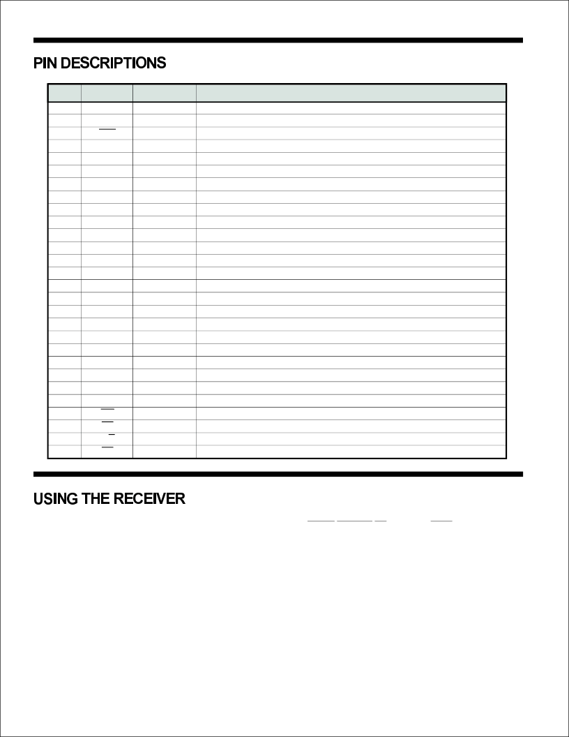
PIN
SYMBOL
FUNCTION
DESCRIPTION
1
2
3
4
5
6
7
8
9
V
WEF
CTS
POWER
OUTPUT
INPUT
INPUT
INPUT
INPUT
OUTPUT
OUTPUT
OUTPUT
OUTPUT
OUTPUT
INPUT
OUTPUT
INPUT
POWER
INPUT
I / O
I / O
I / O
I / O
I / O
I / O
I / O
I / O
INPUT
INPUT
INPUT
INPUT
0.0 Volts
Error indication if high. Status register must be read to determine specific error.
Enables data transmission when low.
Source clock for data transmission. 4 times bit rate.
Hardware feature select.
Master reset, active high.
Low when transmission in progress.
High when data of received word is available.
High when data of a transmitted word may be input.
"Zeroes" data output of transmitter.
"Ones" data output of transmitter.
Source clock for data reception. 4 times bit rate.
First character received flag.
"Zeroes" data input to receiver.
5 Volts ±5%
"Ones" data input to receiver.
Data bus
Data bus
Data bus
Data bus
Data bus
Data bus
Data bus
Data bus
8 bit data bus input control active low.
Chip select, active low.
High for control or status register operations, low for data
8 bit data bus output control, active low.
TXC
HFS
MR
TXE
RXRDY
TXRDY
TXD0
TXD1
RXC
FCR
RXD0
V
RXD1
D0
D1
D2
D3
D4
D5
D6
D7
WE
CS
10
11
12
13
14
15
16
17
18
19
20
21
22
23
24
25
26
27
28
C/
RE
SS
DD
D
HI-6010
The receiver logic is independent of the transmitter except in
thefollowingways:
1.
SelfTest
2.
ParityOption
In self test, the transmitteroutputs route tothe receiverinputs
internally ignoring the external inputs. Also in self test, the
externalreceiverclockisreplacedwiththetransmitterclock.
The parity option affects both the receiver and transmitter.
Eitherbothareoperationalorneither.
WEF is an error indicator.
"underwrite" (failure to keep up with byte loading) and pin 2
It goes high for a transmitter
HARDWARE CONTROL OF THE RECEIVER
PIN 2 - WEF
goes high for any one of three receiver errors. The status
registerwillshowwhichofthethreeerrorsoccurred:
Status Register Bit
SR3
SR4
SR5
Received a parity error
Data Overwritten
Receiving sequence error
The possible Receiver sequence errors are:
1. RXD0 and RXD1 simultaneously a one.
2. Less than 32 bits before 3 nulls.
3. More than 32 bits.
There are no errors flagged for labels received that don't
match stored labels when in the label recognition mode.
ErrorsareclearedbyMRorbyreadingtheStatusRegister.
This pin, along with the control register, sets up the
functioning (e.g. modes) of the chip.
If HFS is low, the
Error
PIN 5 - HFS and the CONTROL REGISTER
HOLT INTEGRATED CIRCUITS
4-4
相關(guān)PDF資料 |
PDF描述 |
|---|---|
| HI-6010CT | ARINC 429 TRANSMITTER/RECEIVER FOR 8 BIT BUS |
| HI-6010J | ARINC 429 TRANSMITTER/RECEIVER FOR 8 BIT BUS |
| HI-6010JF | ARINC 429 TRANSMITTER/RECEIVER FOR 8 BIT BUS |
| HI-6010JTF | ARINC 429 TRANSMITTER/RECEIVER FOR 8 BIT BUS |
| HI-6110 | MIL-STD-1553 / MIL-STD-1760 BC / RT / MT Message Processor |
相關(guān)代理商/技術(shù)參數(shù) |
參數(shù)描述 |
|---|---|
| HI-6010CM-01 | 制造商:HOLTIC 制造商全稱:Holt Integrated Circuits 功能描述:ARINC 429 TRANSMITTER/RECEIVER FOR 8 BIT BUS |
| HI-6010CT | 制造商:Holt Integrated Circuits 功能描述:ARINC 429 Transmitter/Receiver 28-Pin SBCDIP |
| HI-6010J | 制造商:Holt Integrated Circuits 功能描述:ARINC 429 Transmitter/Receiver 28-Pin PLCC |
| HI-6010JF | 制造商:HOLTIC 制造商全稱:Holt Integrated Circuits 功能描述:ARINC 429 TRANSMITTER/RECEIVER FOR 8 BIT BUS |
| HI-6010JT | 制造商:HOLTIC 制造商全稱:Holt Integrated Circuits 功能描述:ARINC 429 TRANSMITTER/RECEIVER FOR 8 BIT BUS |
發(fā)布緊急采購,3分鐘左右您將得到回復(fù)。