- 您現(xiàn)在的位置:買賣IC網(wǎng) > PDF目錄384414 > HI-6010C (HOLT INTEGRATED CIRCUITS INC) 128 MACROCELL 3.3 VOLT ISP CPLD - NOT RECOMMENDED for NEW DESIGN PDF資料下載
參數(shù)資料
| 型號(hào): | HI-6010C |
| 廠商: | HOLT INTEGRATED CIRCUITS INC |
| 元件分類: | 微控制器/微處理器 |
| 英文描述: | 128 MACROCELL 3.3 VOLT ISP CPLD - NOT RECOMMENDED for NEW DESIGN |
| 中文描述: | 1 CHANNEL(S), SERIAL COMM CONTROLLER, CDIP28 |
| 封裝: | ROHS COMPLIANT, SIDE BRAZED, CERAMIC, DIP-28 |
| 文件頁數(shù): | 4/12頁 |
| 文件大小: | 382K |
| 代理商: | HI-6010C |
The transmitter logic is independent of the receiver except in
thefollowingways:
1.
2.
Self Test
Parity Option
In self test the transmitter outputs route to the receiver inputs
internallyandtheTXD0andTXD1outputsareinhibited.
When parity is enabled, both the receiver and transmitter are
affected. Odd parity is automatically generated in the 32nd
bitifthisoptionisselected.
This output goes high for 1 transmitter error and 3 receiver
errors. To determine which error is being flagged, read the
Status Register. Reading the Status Register also clears the
error flag. The transmitter will not function until the error is
cleared. ItcanalsobeclearedbyMRgoinghigh.
Theonlypossibletransmittererrorisgeneratedwhenrunning
in8bitmode. Forthetransmitterthismeansloadingthelast3
bytes while the transmission is in progress. Failure to load a
byte before the previous byte's 8th bit is transmitted will
generatetheerror, indicatedbystatusbitSR7set toa1.
This pin is a hardware gate for transmissions.
transmitter buffer is loaded and Control Register bit CR0 is a
one,theonlyinhibitofthetransmitterwouldbefor
one.
When taken low, transmission of an ARINC word is
enabled. Itmaybepulsedtoreleaseeachtransmittedword.
If the
tobea
The data rate of transmission is controlled by this pin. This
clockmustbe4Xthedesireddaterate.
ThispinalongwiththeControlRegistersetsthefunctioningof
thechip. Forthetransmitter:
HARDWARE CONTROL OF THE TRANSMITTER
PIN 2 - WEF
PIN 3 -
PIN 4 - TXC
PIN 5 - HFS and the CONTROL REGISTER
CTS
CTS
PIN 6 - MR
PIN 7 - TXE
PIN 9 - TXRDY
PIN 10 - TXD0 and PIN 11 - TXD1
The chip is initialized whenever this pin goes high.
Control Register is set to 0X10 0101 (CR7 - CR0). For the
transmitter this sets up 8 bit mode with the transmitter
enabled.
The
Whenever a transmission begins, this pin goes low and
returnshighafterthetransmissioniscomplete.
Whenever TXRDY is a one, data may be written into the
transmitter buffer. In 8 bit "one byte at a time" mode, this pin
maybemonitoredtoindicatewhentowritethenext8bits.
TXD0 will go high during a transmission if the data is zero.
TXD1 goes high if data is a one. When both pins are low this
is referred to as the Null state.
transmitter chip, such as the HI-8382, HI-8383, HI-8585 or
HI-8586 is connected to these pins to translate the 5 volt
levelstotheproperARINCbuslevels.
Typically an ARINC
By writing into the Control Register and reading the Status
Register, the controlling processor can operate the
transmitter independent of the flags at the pins.
TransmissioncanbeinitiatedbychangingCR0froma0toa1
afterthetransmitterbufferhasbeenloaded. ThentheStatus
Registermaybemonitoredasfollows:
SOFTWARECONTROLOFTHETRANSMITTER
Cabling Noise
therefore they are susceptible to noise near ground. If the data
bus is passed by ribbon cable or the equivalent to the device
under test, it is possible to get significant glitches on the Master
Reset line. The problem will appear to be a pattern sensitive
failure. One cure is simply to adequately bypass Master Reset.
AnotheristobuffertheHI-6010inputsnearthechip.
Receiver Seems Dead
receivermustseeawordgapbeforethefirstARINCdatabit.
-The HI-6010 has TTL compatible inputs and
- After Master Reset the HI-6010
Error flags must be cleared by either a Status Register Read or
byaMaster Reset. The operation of either the transmitter or the
receiverisinhibiteduponerror.
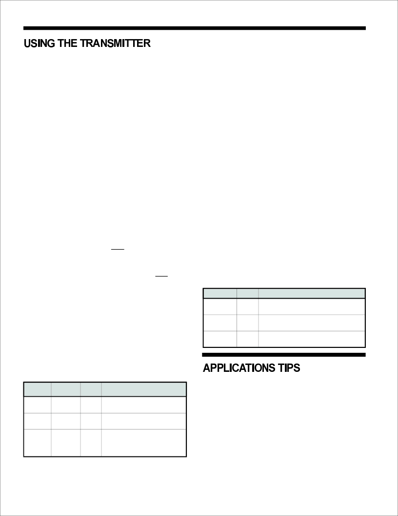
CONTROL
BIT NAME
PROGRAM
VALUE
PIN 5
VALUE
OPERATION
CR0
0
1
X
X
Transmitter is disabled
Transmitter is enabled
CR4
0
1
X
X
Not in self test
Self test enabled
CR5
0
1
0
1
0
0
1
1
8 bit mode + data in 32nd bit
8 bit mode + parity enabled
32 bit mode with parity enabled
8 bit mode with parity enabled
SR0
0
1
Do not load the transmitter buffer
Ready to load the transmitter buffer
SR2
0
1
Transmission in progress
Transmitter is idle
SR7
0
1
No transmission error
8 bit mode only error for underwriting data
STATUS BIT
VALUE
MEANING
HI-6010
HOLT INTEGRATED CIRCUITS
4-6
相關(guān)PDF資料 |
PDF描述 |
|---|---|
| HI-6010CT | ARINC 429 TRANSMITTER/RECEIVER FOR 8 BIT BUS |
| HI-6010J | ARINC 429 TRANSMITTER/RECEIVER FOR 8 BIT BUS |
| HI-6010JF | ARINC 429 TRANSMITTER/RECEIVER FOR 8 BIT BUS |
| HI-6010JTF | ARINC 429 TRANSMITTER/RECEIVER FOR 8 BIT BUS |
| HI-6110 | MIL-STD-1553 / MIL-STD-1760 BC / RT / MT Message Processor |
相關(guān)代理商/技術(shù)參數(shù) |
參數(shù)描述 |
|---|---|
| HI-6010CM-01 | 制造商:HOLTIC 制造商全稱:Holt Integrated Circuits 功能描述:ARINC 429 TRANSMITTER/RECEIVER FOR 8 BIT BUS |
| HI-6010CT | 制造商:Holt Integrated Circuits 功能描述:ARINC 429 Transmitter/Receiver 28-Pin SBCDIP |
| HI-6010J | 制造商:Holt Integrated Circuits 功能描述:ARINC 429 Transmitter/Receiver 28-Pin PLCC |
| HI-6010JF | 制造商:HOLTIC 制造商全稱:Holt Integrated Circuits 功能描述:ARINC 429 TRANSMITTER/RECEIVER FOR 8 BIT BUS |
| HI-6010JT | 制造商:HOLTIC 制造商全稱:Holt Integrated Circuits 功能描述:ARINC 429 TRANSMITTER/RECEIVER FOR 8 BIT BUS |
發(fā)布緊急采購,3分鐘左右您將得到回復(fù)。