- 您現(xiàn)在的位置:買賣IC網(wǎng) > PDF目錄384414 > HI-6110 (Holt Integrated Circuits) MIL-STD-1553 / MIL-STD-1760 BC / RT / MT Message Processor PDF資料下載
參數(shù)資料
| 型號: | HI-6110 |
| 廠商: | Holt Integrated Circuits |
| 英文描述: | MIL-STD-1553 / MIL-STD-1760 BC / RT / MT Message Processor |
| 中文描述: | 符合MIL - STD - 1553 /符合MIL - STD - 1760年/放射/噸消息處理器 |
| 文件頁數(shù): | 2/36頁 |
| 文件大小: | 532K |
| 代理商: | HI-6110 |
第1頁當(dāng)前第2頁第3頁第4頁第5頁第6頁第7頁第8頁第9頁第10頁第11頁第12頁第13頁第14頁第15頁第16頁第17頁第18頁第19頁第20頁第21頁第22頁第23頁第24頁第25頁第26頁第27頁第28頁第29頁第30頁第31頁第32頁第33頁第34頁第35頁第36頁
HOLT INTEGRATED CIRCUITS
2
HI-6110
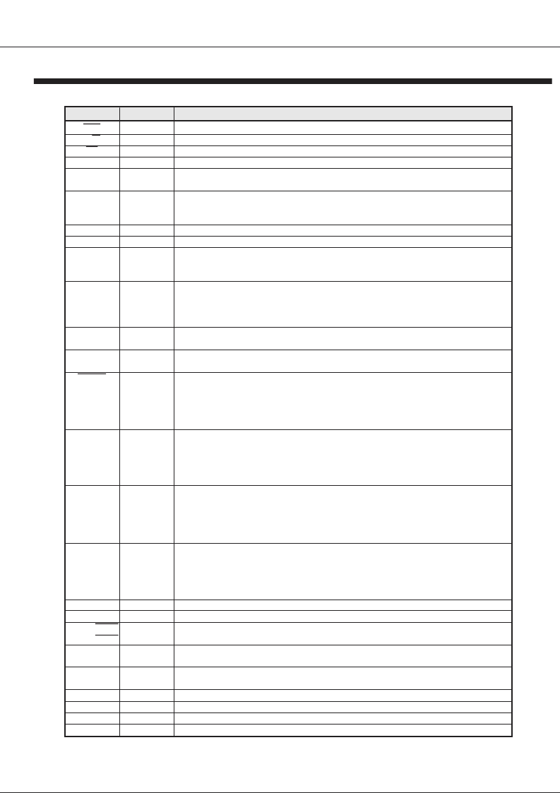
PIN DESCRIPTIONS
SIGNAL
STR
R/
CS
FUNCTION
INPUT
INPUT
INPUT
I/O
INPUTS
DESCRIPTION
During I/O operations, data is latched on rising edge.
Device register access, READ = 1, WRITE = 0. (12K ohm pull-up resistor)
Chip Select for register reads and writes, active low. (12K ohm pull-down resistor)
Data bus signals. (12K ohm pull-down resistors)
Register access address, inputs are ORed with corresponding Control register bits.
(12K ohm pull-down resistors)
Message starts on rising edge when in BC mode. Input is ORed with a corresponding
Control register bit, where a 0 to 1 transition will also trigger message start. (This input
has a 12K ohm pull-down resistor.)
System Clock. (12K ohm pull-down resistor)
up
GND
MR
Power supply Ground, 0V.
Master
eset, active high. Clears all data FIFOs and all registers except the Control,
Transmit Status Word and Transmit Mode Data Word registers. This i
.
oes high
error is
resets
BCSTART is asserted to begin
and MT
output signal mirro
corresponding Status register bit.
Goes high at the end of a valid message sequence.
corresponding Status register bit.
When low, data is available in the receive data FIFO for the active bus. This output
signal mirrors a corresponding Status register bit.
Flag for register writes of received message words other than Data words.
In BC mode: Goes low when a Status Word register is written.
In RT or MT mode: Goes low when either a Command word, Status word, or Mode
data word register is received and written in a register. This output mirrors a
corresponding Status register bit.
RF0 function: If a “1” when reading Bus A Word or Bus B Word registers, the stored
word had data sync.
RCVCMDA function: In RT mode or MT mode, RCVCMDA goes high when a valid
receive command has been decoded on Bus A.
This output mirrors a corresponding Status register bit.
RF1 function: If a “1” when reading Bus A Word or Bus B Word registers, the stored
word had command sync.
RCVCMDB function: In RT mode or MT mode, RCVCMDB goes high when a valid
receive command has been decoded on Bus B.
This output mirrors a corresponding Status register bit.
Receive A and Receive B flags: In BC mode, these signals go high when any valid
word is received on Bus A or Bus B.
In RT or MT mode, these signals go high when a valid command is received on Bus A
or Bus B. For valid RT-to-RT only, RCV goes high after command word pair. These
output signals mirror two corresponding Status register bits.
Logic one disables the Bus A transmitter. (12K ohm pull-up resistor)
Logic one disables the Bus B transmitter. (12K ohm pull-up resistor)
Positive and negative polarity of 1553 signals for Buses A and B. These signal pairs
connect the analog transceivers to the external transformer.
Selects operating mode. This input signal is ORed with a corresponding
Control register bit. (12K ohm pull-up resistor)
Selects operating mode. This input signal is ORed with a corresponding
Control register bit. (12K ohm pull-down resistor)
Remote Terminal address inputs, for RT mode. (12K ohm pull-up resistors)
This input sets Remote Terminal address parity, odd. (12K ohm pull-down resistor)
+3.3VDC ±5% power supply input for internal logic
+3.3VDC ±5% power supply inputs for Bus A and Bus B transceivers
ERROR
OUT
next message.
VALMESS
OUTPUT
signal
(12K ohm pull-
resistor)
D0 - D15
RA0 - RA3
BCSTART
INPUT
CLK
INPUT
POWER
INPUT
R
nput is ORed
with a corresponding Control register bit (12K ohm pull-down resistor)
ERROR g
when a message
In BC mode, ERROR
when
For RT
modes ERROR resets automatically after 3 to 4uS.
This
rs a
PUT
detected.
the
This output
mirrors a
FFEMPTY
OUTPUT
OUTPUT
RF0 /
RCVCMDA
OUTPUT
RF1 /
RCVCMDB
OUTPUT
RCVA
RCVB
OUTPUTS
TXINHA
TXINHB
BUSA,
BUSB,
BCMODE
INPUT
INPUT
XFMR
INPUT
RTMODE
INPUT
RTA0-RTA4
RTAP
VDDLOG
VDDA, VDDB
INPUTS
INPUT
POWER
POWER
W
RFLAG
BUSA
BUSB
相關(guān)PDF資料 |
PDF描述 |
|---|---|
| HI-6110PQI | MIL-STD-1553 / MIL-STD-1760 BC / RT / MT Message Processor |
| HI-6110PQIF | MIL-STD-1553 / MIL-STD-1760 BC / RT / MT Message Processor |
| HI-6110PQM | MIL-STD-1553 / MIL-STD-1760 BC / RT / MT Message Processor |
| HI-6110PQMF | MIL-STD-1553 / MIL-STD-1760 BC / RT / MT Message Processor |
| HI-6110PQT | MIL-STD-1553 / MIL-STD-1760 BC / RT / MT Message Processor |
相關(guān)代理商/技術(shù)參數(shù) |
參數(shù)描述 |
|---|---|
| HI-6110_10 | 制造商:HOLTIC 制造商全稱:Holt Integrated Circuits 功能描述:MIL-STD-1553 / MIL-STD-1760 MIL-STD-1553 / MIL-STD-1760 |
| HI-6110PCI | 制造商:HOLTIC 制造商全稱:Holt Integrated Circuits 功能描述:MIL-STD-1553 / MIL-STD-1760 BC / RT / MT Message Processor |
| HI-6110PCIF | 制造商:HOLTIC 制造商全稱:Holt Integrated Circuits 功能描述:MIL-STD-1553 / MIL-STD-1760 BC / RT / MT Message Processor |
| HI-6110PCM | 制造商:HOLTIC 制造商全稱:Holt Integrated Circuits 功能描述:MIL-STD-1553 / MIL-STD-1760 BC / RT / MT Message Processor |
| HI-6110PCMF | 制造商:HOLTIC 制造商全稱:Holt Integrated Circuits 功能描述:MIL-STD-1553 / MIL-STD-1760 BC / RT / MT Message Processor |
發(fā)布緊急采購,3分鐘左右您將得到回復(fù)。