- 您現(xiàn)在的位置:買賣IC網(wǎng) > PDF目錄384414 > HI-6110 (Holt Integrated Circuits) MIL-STD-1553 / MIL-STD-1760 BC / RT / MT Message Processor PDF資料下載
參數(shù)資料
| 型號: | HI-6110 |
| 廠商: | Holt Integrated Circuits |
| 英文描述: | MIL-STD-1553 / MIL-STD-1760 BC / RT / MT Message Processor |
| 中文描述: | 符合MIL - STD - 1553 /符合MIL - STD - 1760年/放射/噸消息處理器 |
| 文件頁數(shù): | 5/36頁 |
| 文件大小: | 532K |
| 代理商: | HI-6110 |
第1頁第2頁第3頁第4頁當(dāng)前第5頁第6頁第7頁第8頁第9頁第10頁第11頁第12頁第13頁第14頁第15頁第16頁第17頁第18頁第19頁第20頁第21頁第22頁第23頁第24頁第25頁第26頁第27頁第28頁第29頁第30頁第31頁第32頁第33頁第34頁第35頁第36頁
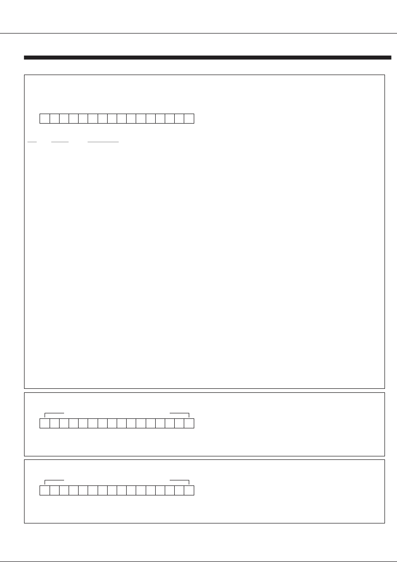
TRANSMIT DATA FIFO (Write only) Write Address: X010
MIL-STD-1553 Message Data Word 15:0
15 14 13 12 11 10
9
8
7
6
5
4
3
2
1
0
MSB
LSB
RECEIVE DATA FIFO (Read only) Read Address: 0100
MIL-STD-1553 Message Data Word 15:0
15 14 13 12 11 10
9
8
7
6
5
4
3
2
1
0
MSB
LSB
RA3
RA2
RA1
RA0
TRB
TRA
RTBCBCSTART
MR
MSB
LSB
15 14 13 12 11 10
9
8
7
6
5
4
3
2
1
0
1
0
X
X
X
NoRENo Used
0
REGISTER FORMATS (BC Mode)
HI-6110 (BUS CONTROLLER MODE)
CONTROL REGISTER (R/W) Write Address: X1XX, Read Address: 1100
The Control Register settings determine HI-6110 operating
mode,clockfrequencyandthebusenabledfortransmit.Itcan
also be used to address registers for read/write operations, to
assert master reset, and to initiate MIL-STD-1553 message
sequences.
The Transmit Data FIFO is 32-words deep and holds MIL-
STD-1553 message data. The FIFO is cleared on Master
Reset.
Message data to be transmitted by the BC may be loaded into
the TRANSMIT DATA FIFO by the host prior to BCSTART.
Any data word must be loaded before mid-parity bit for the
1553 word it follows. Words are transmitted in the order they
areloaded.
The Receive Data FIFO is 32-words deep and holds MIL-
STD-1553 message data. The FIFO is cleared by Master
ResetorwhenBCSTARToccurs.
AllMIL-STD-1553datawordsreceivedbytheBCarestoredin
the Receive DATA FIFO. A low FFEMPTY flag (output pin or
Status register bit) means message data is available to be
read by the host. Successive data reads cause FFEMPTY to
gohighwhenthelastwordisread.
HOLT INTEGRATED CIRCUITS
5
BIT
15
14
NAME
-
REPTO
FUNCTION
NotusedinBCmode
Controlsthetime-outwhichcausestheNoResponseError.
0
17usecGap(equivalentto57usecfor5.2.1.7oftheRTValidationTestPlan)
1
131usecGap
NotusedinBCmode
SelectsthefrequencyoftheHI-6110externalCLKinput,asfollows:
CLKSEL
Value
0
24MHz
1
12MHz
Thisbitmustbewrittento“0”.
13
12
-
CLKSEL
10-7
RA3:0
Register Address for HI-6110 register and data read and write operations. The register address is defined by
the logical OR of these bits and their corresponding input pins. Writting Control Register bits 10:7 to 0000 is
necessaryiftheRA0-RA3inputpinsareusedforHI-6110registeraddressing.
NotusedinBCmode
Setting either TRA or TRB to "1" enables transmit on MIL-STD-1553 BUS A or BUS B. Setting both TRA and
TRB selects neither bus. The
protocol engine connects to the selected, active bus. The 1553 receiver,
Manchester ecoder and RCV output signal are still operational on the inactive bus. Valid words received on the
inactive bus can be read without changing active bus by reading the Bus A Word or Bus B Word register.
NOTE:
heTXINHAandTXINHBinputpinscanoverridebusenablement.
6
5-4
-
TRB,TRA
BC
T
3-2
RTMODE,
BCMODE
HI-6110modeselectbits.TheseControlRegisterbitsarelogicallyOR'edwiththeircorrespondinginputpins,
allowingtheusertoselect1553operatingmodeundereitherhardwareorsoftwarecontrol:
RTMODE
BCMODE
1553OPERATINGMODE
0
0
BusMonitor(MT),withassignedRTaddress
0
1
BusController(BC)
1
0
RemoteTerminal(RT)
1
1
BusMonitor(MT),withoutassignedRTaddress
If initially reset, writing a "1" to this bit initiates a BC message sequence. This bit should be reset before next
message.
Master Reset. Writing "1" and then “0” to this bit performs the same function as pulsing the MR pin. All register
and data FIFOs are cleared when master reset is asserted. The Control Register is the exception; it is not
affectedbyMasterReset.
11
Reserved
1
BCSTART
0
MR
相關(guān)PDF資料 |
PDF描述 |
|---|---|
| HI-6110PQI | MIL-STD-1553 / MIL-STD-1760 BC / RT / MT Message Processor |
| HI-6110PQIF | MIL-STD-1553 / MIL-STD-1760 BC / RT / MT Message Processor |
| HI-6110PQM | MIL-STD-1553 / MIL-STD-1760 BC / RT / MT Message Processor |
| HI-6110PQMF | MIL-STD-1553 / MIL-STD-1760 BC / RT / MT Message Processor |
| HI-6110PQT | MIL-STD-1553 / MIL-STD-1760 BC / RT / MT Message Processor |
相關(guān)代理商/技術(shù)參數(shù) |
參數(shù)描述 |
|---|---|
| HI-6110_10 | 制造商:HOLTIC 制造商全稱:Holt Integrated Circuits 功能描述:MIL-STD-1553 / MIL-STD-1760 MIL-STD-1553 / MIL-STD-1760 |
| HI-6110PCI | 制造商:HOLTIC 制造商全稱:Holt Integrated Circuits 功能描述:MIL-STD-1553 / MIL-STD-1760 BC / RT / MT Message Processor |
| HI-6110PCIF | 制造商:HOLTIC 制造商全稱:Holt Integrated Circuits 功能描述:MIL-STD-1553 / MIL-STD-1760 BC / RT / MT Message Processor |
| HI-6110PCM | 制造商:HOLTIC 制造商全稱:Holt Integrated Circuits 功能描述:MIL-STD-1553 / MIL-STD-1760 BC / RT / MT Message Processor |
| HI-6110PCMF | 制造商:HOLTIC 制造商全稱:Holt Integrated Circuits 功能描述:MIL-STD-1553 / MIL-STD-1760 BC / RT / MT Message Processor |
發(fā)布緊急采購,3分鐘左右您將得到回復(fù)。