- 您現(xiàn)在的位置:買(mǎi)賣(mài)IC網(wǎng) > PDF目錄384422 > HIP6021CBZ (INTERSIL CORP) Advanced PWM and Triple Linear Power Controller PDF資料下載
參數(shù)資料
| 型號(hào): | HIP6021CBZ |
| 廠商: | INTERSIL CORP |
| 元件分類(lèi): | 穩(wěn)壓器 |
| 英文描述: | Advanced PWM and Triple Linear Power Controller |
| 中文描述: | SWITCHING CONTROLLER, 215 kHz SWITCHING FREQ-MAX, PDSO28 |
| 封裝: | GREEN, PLASTIC, SOIC-28 |
| 文件頁(yè)數(shù): | 12/15頁(yè) |
| 文件大小: | 341K |
| 代理商: | HIP6021CBZ |
第1頁(yè)第2頁(yè)第3頁(yè)第4頁(yè)第5頁(yè)第6頁(yè)第7頁(yè)第8頁(yè)第9頁(yè)第10頁(yè)第11頁(yè)當(dāng)前第12頁(yè)第13頁(yè)第14頁(yè)第15頁(yè)
12
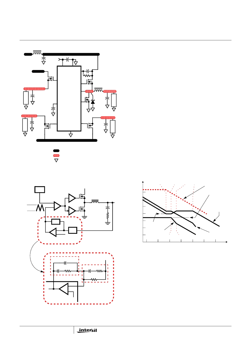
Compensation Break Frequency Equations
Figure 10 shows an asymptotic plot of the DC-DC
converter’s gain vs. frequency. The actual Modulator Gain
has a high gain peak dependent on the quality factor (Q) of
the output filter, which is not shown in Figure 9. Using the
above guidelines should yield a Compensation Gain similar
to the curve plotted. The open loop error amplifier gain
bounds the compensation gain. Check the compensation
gain at F
P2
with the capabilities of the error amplifier. The
Closed Loop Gain is constructed on the log-log graph of
Figure 10 by adding the Modulator Gain (in dB) to the
Compensation Gain (in dB). This is equivalent to multiplying
the modulator transfer function to the compensation transfer
function and plotting the gain.
The compensation gain uses external impedance networks
Z
FB
and Z
IN
to provide a stable, high bandwidth (BW) overall
loop. A stable control loop has a gain crossing with
-20dB/decade slope and a phase margin greater than 45
degrees. Include worst case component variations when
determining phase margin.
Component Selection Guidelines
Output Capacitor Selection
The output capacitors for each output have unique
requirements. In general, the output capacitors should be
selected to meet the dynamic regulation requirements.
Additionally, the PWM converters require an output capacitor
to filter the current ripple. The load transient for the
microprocessor core requires high quality capacitors to
supply the high slew rate (di/dt) current demands.
FIGURE 8. PRINTED CIRCUIT BOARD POWER PLANES AND
ISLANDS
V
OUT1
Q1
L
OUT1
Q2
Q3
Q4
C
SS
+12V
C
VCC
VIA CONNECTION TO GROUND PLANE
ISLAND ON POWER PLANE LAYER
ISLAND ON CIRCUIT PLANE LAYER
C
OUT1
CR1
HIP6021
C
IN
C
OUT2
V
OUT2
V
OUT3
+5V
IN
SS
PGND
LGATE1
UGATE1
PHASE1
DRIVE3
KEY
GND
OCSET1
VCC
DRIVE2
R
OCSET1
C
OCSET1
L
V
OUT4
DRIVE4
+3.3V
IN
L
IN
Q5
C
OUT3
C
OUT4
L
L
L
+3.3V
IN
FIGURE 9. VOLTAGE-MODE BUCK CONVERTER
COMPENSATION DESIGN
V
OUT
OSC
REFERENCE
L
O
C
O
ESR
V
IN
V
OSC
ERROR
AMP
PWM
COMP
DRIVER
(PARASITIC)
Z
FB
+
-
DACOUT
R1
R3
R2
C3
C2
C1
COMP
V
OUT
FB
Z
FB
HIP6021
Z
IN
DRIVER
DETAILED COMPENSATION COMPONENTS
PHASE
V
E/A
+
-
+
-
Z
IN
F
Z1
-----------------------------------
=
F
Z2
R3
)
C3
×
------------------------+
=
F
P1
2
π
R
2
+
----------------------
×
×
------------------------------------------------------
=
F
P2
-----------------------------------
=
FIGURE 10. ASYMPTOTIC BODE PLOT OF CONVERTER GAIN
100
80
60
40
20
0
-20
-40
-60
F
P1
F
Z2
10M
1M
100K
10K
1K
100
10
OPEN LOOP
ERROR AMP GAIN
F
Z1
F
P2
F
LC
F
ESR
COMPENSATION
GAIN
G
FREQUENCY (Hz)
MODULATOR
GAIN
CLOSED LOOP
GAIN
20
------------
log
20
-------
log
HIP6021
相關(guān)PDF資料 |
PDF描述 |
|---|---|
| HIP6200 | Transient Voltage Regulator(瞬變電壓穩(wěn)壓器) |
| HIP6201 | Transient Voltage Regulator(瞬變電壓穩(wěn)壓器) |
| HIP6200CB | Transient Voltage Regulator DeCAPitator⑩ |
| HIP6201CB | Transient Voltage Regulator DeCAPitator⑩ |
| HIP6301CBZ | Microprocessor CORE Voltage Regulator Multi-Phase Buck PWM Controller |
相關(guān)代理商/技術(shù)參數(shù) |
參數(shù)描述 |
|---|---|
| HIP6021CBZ-T | 功能描述:電壓模式 PWM 控制器 SINGLE PWM & TRPL LINEAR CNTRLR RoHS:否 制造商:Texas Instruments 輸出端數(shù)量:1 拓?fù)浣Y(jié)構(gòu):Buck 輸出電壓:34 V 輸出電流: 開(kāi)關(guān)頻率: 工作電源電壓:4.5 V to 5.5 V 電源電流:600 uA 最大工作溫度:+ 125 C 最小工作溫度:- 40 C 封裝 / 箱體:WSON-8 封裝:Reel |
| HIP6021EVAL1 | 功能描述:電源管理IC開(kāi)發(fā)工具 HIP6021 EVAL BRD RoHS:否 制造商:Maxim Integrated 產(chǎn)品:Evaluation Kits 類(lèi)型:Battery Management 工具用于評(píng)估:MAX17710GB 輸入電壓: 輸出電壓:1.8 V |
| HIP6028 | 制造商:INTERSIL 制造商全稱:Intersil Corporation 功能描述:Advanced PWM and Dual Linear Power Control with Integrated ACPI Support Interface |
| HIP6028CB | 制造商:Rochester Electronics LLC 功能描述:- Bulk |
| HIP6028CB WAF | 制造商:Harris Corporation 功能描述: |
發(fā)布緊急采購(gòu),3分鐘左右您將得到回復(fù)。