- 您現(xiàn)在的位置:買賣IC網(wǎng) > PDF目錄384422 > HIP6201CB (INTERSIL CORP) Transient Voltage Regulator DeCAPitator⑩ PDF資料下載
參數(shù)資料
| 型號(hào): | HIP6201CB |
| 廠商: | INTERSIL CORP |
| 元件分類: | 模擬信號(hào)調(diào)理 |
| 英文描述: | Transient Voltage Regulator DeCAPitator⑩ |
| 中文描述: | SPECIALTY ANALOG CIRCUIT, PDSO8 |
| 封裝: | PLASTIC, MS-012-AA, SOIC-8 |
| 文件頁(yè)數(shù): | 4/9頁(yè) |
| 文件大小: | 87K |
| 代理商: | HIP6201CB |
2-444
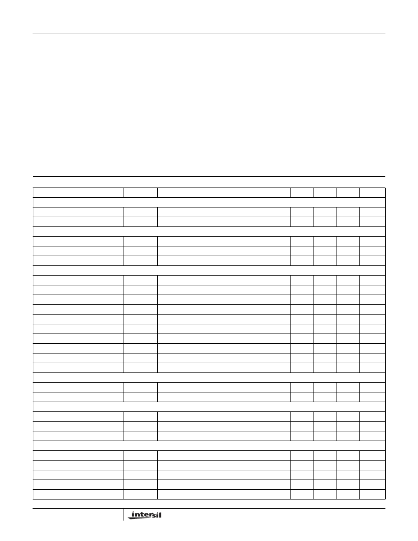
Absolute Maximum Ratings
Thermal Information
Supply Voltage, V
CC
, P
VCC
. . . . . . . . . . . . . . . . . . . . . . . . . . . +7.0V
EN, CAP, OUT, SNS. . . . . . . . . . . . . . . . . . . . . . . .GND-0.3V to +7V
GND - PGND . . . . . . . . . . . . . . . . . . . . . . . . . . . . . . . -0.5V to +0.5V
Operating Conditions
Supply Voltage, V
CC
. . . . . . . . . . . . . . . . . . . . . . . . . . . . . +5V
±
5%
Output Device Supply Voltage, P
VCC
. . . . . . . . . . . .+4.5V to +5.5V
Output Voltage, OUT = SNS = CAP. . . . . . . . . . . . . .+1.3V to +2.0V
. . . . . . . . . . . . . . . . . . . . . . . . . . . . . . . . . . . ±
8A
Ambient Operating Temperature Range . . . . . . . . . . . .0
o
C to 70
o
C
Junction Temperature Range. . . . . . . . . . . . . . . . . . . .0
o
C to 125
o
C
Thermal Resistance (Typical, Note 1)
SOIC Package . . . . . . . . . . . . . . . . . . . . . . . . . . . . .
Maximum Junction Temperature . . . . . . . . . . . . . . . . . . . . . . .150
o
C
Maximum Storage Temperature Range. . . . . . . . . . -65
o
C to 150
o
C
Maximum Lead Temperature (Soldering 10s) . . . . . . . . . . . . .300
o
C
(SOIC - Lead Tips Only)
θ
JA
(
o
C/W)
145
o
C/W
CAUTION: Stresses above those listed in “Absolute Maximum Ratings” may cause permanent damage to the device. This is a stress only rating and operation of the
device at these or any other conditions above those indicated in the operational sections of this specification is not implied.
NOTE:
1.
θ
JA
is measured with the component mounted on an evaluation PC board in free air.
Electrical Specifications
Recommended Operating Conditions, Unless Otherwise Noted
PARAMETER
SYMBOL
TEST CONDITIONS
MIN
TYP
MAX
UNITS
V
CC
SUPPLY CURRENT
Nominal Supply
I
VCC
I
VCC_SD
-
300
-
μ
A
μ
A
Shutdown Supply
EN = GND
-
1
-
PROTECTION CIRCUITRY
EN Threshold
V
TH_EN
OT
0.8
1.5
2.0
V
o
C
Overtemperature (OT) Threshold
130
150
170
On-Resistance of OT NMOS
R
ds_TFN
-
250
600
POWER-ON RESET (POR)
V
CC
Rising Threshold
V
CC
Falling Threshold
CAP Rising Threshold
V
THH_VCC
V
THL_VCC
V
TH_CAP
EN = V
CC
EN = V
CC
EN = V
CC
EN = V
CC
-
4.1
4.5
V
3.6
4.0
-
V
-
1.10
1.20
V
CAP Falling Threshold
0.95
1.05
-
V
POR Turn-Off Delay to EN Falling
-
2
-
μ
s
POR Turn-On Delay to EN Rising
-
1
-
ms
POR Turn-Off Delay to V
CC
UV
POR Turn-On Delay after V
CC
UV
POR Turn-Off Delay to CAP UV
EN = V
CC
, V
CC
Falling
EN = V
CC
, V
CC
Rising
EN = V
CC
, CAP Falling
EN = V
CC
, CAP Rising
-
15
-
μ
s
μ
s
μ
s
μ
s
-
15
-
-
2
-
POR Turn-On Delay after CAP UV
-
15
-
REFERENCE VOLTAGE
V
SNS
- V
CAP
V
CAP
- V
SNS
AMPLIFIERS
V
HIGH
V
LOW
CAP = 2V, SNS Increased Until Amplifier Turns On
-
30
-
mV
CAP = 2V, SNS Decreased Until Amplifier Turns On
-
20
-
mV
Transconductance
-
500
-
A/V
Response Time (Rising)
60mV Step on OUT, Time for I
OUT
< -4A
-60mV Step on OUT, Time for I
OUT
> 4A
50
100
175
ns
Response Time (Falling)
50
100
175
ns
RESISTOR VALUES
Small Time Constant Resistor
R
T1
R
T2
R
VCC
R
OUT
R
GND
120
200
250
Large Time Constant Resistor
3000
4000
5500
V
CC
to P
VCC
Resistor
OUT to SNS Resistor
6
10
16
1000
1500
2100
GND to PGND Resistors
-
140
-
HIP6200, HIP6201
相關(guān)PDF資料 |
PDF描述 |
|---|---|
| HIP6301CBZ | Microprocessor CORE Voltage Regulator Multi-Phase Buck PWM Controller |
| HIP6301CBZA-T | Microprocessor CORE Voltage Regulator Multi-Phase Buck PWM Controller |
| HIP6301CBZ-T | Microprocessor CORE Voltage Regulator Multi-Phase Buck PWM Controller |
| HIP6301EVAL2 | Microprocessor CORE Voltage Regulator Multi-Phase Buck PWM Controller |
| HIP6301 | Microprocessor CORE Voltage Regulator Multi-Phase Buck PWM Controller(微處理器核心電壓穩(wěn)壓多相沖跳脈寬調(diào)制控制器) |
相關(guān)代理商/技術(shù)參數(shù) |
參數(shù)描述 |
|---|---|
| HIP6201CB WAF | 制造商:Harris Corporation 功能描述: |
| HIP6211 | 制造商:未知廠家 制造商全稱:未知廠家 功能描述:Dual Low Noise LDO in 3mm】3mm MLF⑩ |
| HIP6211-15UZ | 制造商:未知廠家 制造商全稱:未知廠家 功能描述:Dual Low Noise LDO in 3mm】3mm MLF⑩ |
| HIP6211-15VZ | 制造商:未知廠家 制造商全稱:未知廠家 功能描述:Dual Low Noise LDO in 3mm】3mm MLF⑩ |
| HIP6211-18UZ | 制造商:未知廠家 制造商全稱:未知廠家 功能描述:Dual Low Noise LDO in 3mm】3mm MLF⑩ |
發(fā)布緊急采購(gòu),3分鐘左右您將得到回復(fù)。