- 您現(xiàn)在的位置:買賣IC網(wǎng) > PDF目錄384465 > HY29LV320TT-12I (HYNIX SEMICONDUCTOR INC) 150 x 32 pixel format, LED Backlight available PDF資料下載
參數(shù)資料
| 型號: | HY29LV320TT-12I |
| 廠商: | HYNIX SEMICONDUCTOR INC |
| 元件分類: | DRAM |
| 英文描述: | 150 x 32 pixel format, LED Backlight available |
| 中文描述: | 2M X 16 FLASH 3V PROM, 120 ns, PDSO48 |
| 封裝: | TSOP-48 |
| 文件頁數(shù): | 17/44頁 |
| 文件大?。?/td> | 323K |
| 代理商: | HY29LV320TT-12I |
第1頁第2頁第3頁第4頁第5頁第6頁第7頁第8頁第9頁第10頁第11頁第12頁第13頁第14頁第15頁第16頁當前第17頁第18頁第19頁第20頁第21頁第22頁第23頁第24頁第25頁第26頁第27頁第28頁第29頁第30頁第31頁第32頁第33頁第34頁第35頁第36頁第37頁第38頁第39頁第40頁第41頁第42頁第43頁第44頁
1
r
H
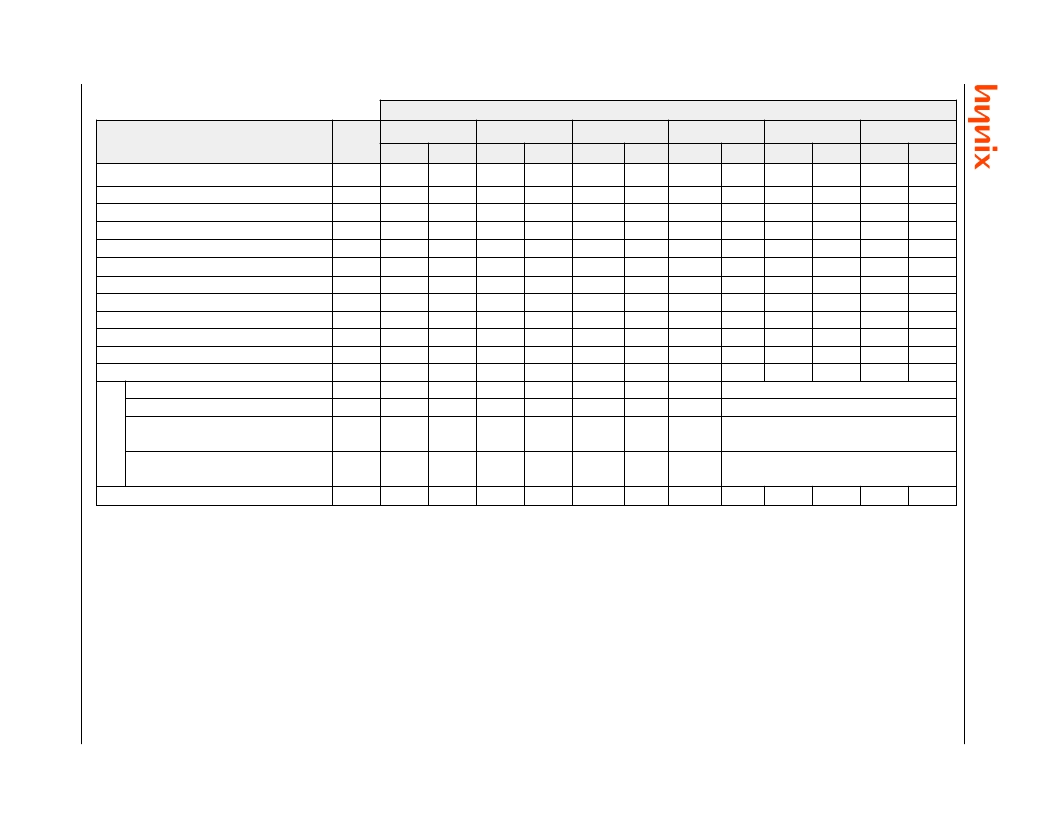
Table 9. HY29LV320 Command Sequences
s
e
y
C
s
u
d
B
r
h
4
,
,
,
e
c
n
e
u
q
e
S
d
n
a
m
m
o
C
e
W
e
y
C
s
t
r
F
d
a
D
n
o
c
e
S
d
T
d
h
D
t
u
o
F
d
d
h
D
t
F
d
h
D
t
S
d
d
d
A
a
D
d
A
d
A
a
D
A
a
d
A
a
d
A
a
d
a
e
R
0
A
R
D
R
t
s
e
r
E
t
E
r
N
o
U
o
U
o
U
p
C
r
e
S
a
E
a
E
R
7
1
3
4
4
3
2
2
6
6
1
1
3
3
X
5
5
5
5
X
X
5
5
X
X
5
5
X
5
5
5
5
X
X
5
5
X
X
5
5
X
5
5
5
5
X
X
5
5
X
X
5
5
0
A
A
A
A
0
0
A
A
0
0
A
A
F
A
A
A
A
9
A
A
A
B
3
A
A
c
e
c
P
B
B
B
a
E
E
S
e
R
e
M
D
S
e
2
n
o
e
R
o
e
R
a
o
s
a
p
y
s
a
p
y
s
a
p
y
e
s
e
s
a
e
p
s
u
m
u
s
e
r
a
n
a
e
c
e
A
A
A
A
X
A
A
A
A
A
A
A
A
X
P
2
2
2
2
2
2
X
5
5
5
5
0
D
5
5
5
5
5
5
0
P
5
5
5
5
5
5
5
5
5
5
5
5
5
5
8
0
0
0
8
9
A
2
S
l
m
c
c
c
2
n
X
A
X
P
X
0
D
0
P
m
s
s
s
k
k
k
t
s
a
o
P
e
R
6
m
5
5
5
5
5
5
5
0
0
8
8
5
5
5
5
5
5
A
A
A
A
A
A
A
A
2
2
5
5
5
5
5
5
5
S
0
0
1
3
9
A
A
d
e
n
s
s
7
8
e
d
o
C
A
A
A
A
2
2
5
5
5
5
5
5
5
5
5
5
0
0
9
9
0
1
0
0
X
X
X
X
X
X
D
A
0
o
B
X
X
X
X
0
e
d
o
C
E
7
2
2
=
t
o
B
p
o
r
e
r
e
T
,
D
d
S
7
2
2
e
d
=
t
o
e
n
U
e
P
B
m
=
0
0
1
0
y
V
t
e
P
r
e
S
3
5
5
5
A
A
A
A
2
5
5
5
5
5
0
9
2
0
X
)
A
S
(
S
e
=
c
e
S
2
t
B
r
c
n
n
o
e
R
3
5
5
5
A
A
A
A
2
5
5
5
5
5
0
9
3
0
X
X
X
y
a
y
d
e
k
c
a
o
d
e
k
c
o
d
n
a
d
d
e
n
a
e
e
T
O
e
P
N
=
=
0
0
0
8
X
X
X
X
d
y
u
Q
)
F
C
(
e
c
a
h
s
a
n
o
m
m
o
C
0
1
1
5
5
X
X
X
8
9
E
Legend:
X = Don
’
t Care
PA/PD = Memory address/data for the program operation
RA/RD = Memory address/data for the read operation
SA = A[20:12], sector address of the sector to be erased or verified (see Tables 1 and 2).
Notes:
1. All values are in hexadecimal.
2. All bus cycles are write operations except all cycles of the Read command and the fourth cycle of Electronic ID command.
3. Data bits DQ[15:8] are don
’
t cares except for
‘
PD
’
in program cycles.
4. Address is A[10:0]. Other (upper) address bits are don
’
t cares except when
‘
SA
’
or
‘
PA
’
is required.
5. The Unlock Bypass command is required prior to the Unlock Bypass Program command.
6. The Unlock Bypass Reset command is valid only while the device is in the Unlock Bypass mode.
7. The Erase Suspend command is valid only during a sector erase operation. The system may read and program in non-erasing sectors, or enter the Electronic
ID mode, while in the Erase Suspend mode.
8. The Erase Resume command is valid only during the Erase Suspend mode.
9. Multiple sectors may be specified for erasure. See command description.
10.See CFI section of specification for additional information.
11.See Electronic ID section of specification for additional information.
相關PDF資料 |
PDF描述 |
|---|---|
| HY57V283220LT-5 | 4 Banks x 1M x 32Bit Synchronous DRAM |
| HY57V283220LT-55 | 4 Banks x 1M x 32Bit Synchronous DRAM |
| HY57V283220LT-6 | 4 Banks x 1M x 32Bit Synchronous DRAM |
| HY57V283220LT-7 | 4 Banks x 1M x 32Bit Synchronous DRAM |
| HY57V283220LT-8 | 4 Banks x 1M x 32Bit Synchronous DRAM |
相關代理商/技術參數(shù) |
參數(shù)描述 |
|---|---|
| HY29LV320TT-70 | 制造商:HYNIX 制造商全稱:Hynix Semiconductor 功能描述:32 Mbit (2M x 16) Low Voltage Flash Memory |
| HY29LV320TT-70I | 制造商:HYNIX 制造商全稱:Hynix Semiconductor 功能描述:32 Mbit (2M x 16) Low Voltage Flash Memory |
| HY29LV320TT-80 | 制造商:HYNIX 制造商全稱:Hynix Semiconductor 功能描述:32 Mbit (2M x 16) Low Voltage Flash Memory |
| HY29LV320TT-80I | 制造商:HYNIX 制造商全稱:Hynix Semiconductor 功能描述:32 Mbit (2M x 16) Low Voltage Flash Memory |
| HY29LV320TT-90 | 制造商:HYNIX 制造商全稱:Hynix Semiconductor 功能描述:32 Mbit (2M x 16) Low Voltage Flash Memory |
發(fā)布緊急采購,3分鐘左右您將得到回復。