- 您現(xiàn)在的位置:買賣IC網(wǎng) > PDF目錄379204 > IBM13M32734JCA (IBM Microeletronics) 32M x 72 Two Bank Registered/Buffered SDRAM Module(64M x 64 2組不帶緩沖同步動(dòng)態(tài)RAM模塊) PDF資料下載
參數(shù)資料
| 型號(hào): | IBM13M32734JCA |
| 廠商: | IBM Microeletronics |
| 英文描述: | 32M x 72 Two Bank Registered/Buffered SDRAM Module(64M x 64 2組不帶緩沖同步動(dòng)態(tài)RAM模塊) |
| 中文描述: | 32M × 72配置兩個(gè)銀行的注冊(cè)/緩沖內(nèi)存模組(64米× 64 2組不帶緩沖同步動(dòng)態(tài)內(nèi)存模塊) |
| 文件頁(yè)數(shù): | 5/20頁(yè) |
| 文件大?。?/td> | 529K |
| 代理商: | IBM13M32734JCA |
第1頁(yè)第2頁(yè)第3頁(yè)第4頁(yè)當(dāng)前第5頁(yè)第6頁(yè)第7頁(yè)第8頁(yè)第9頁(yè)第10頁(yè)第11頁(yè)第12頁(yè)第13頁(yè)第14頁(yè)第15頁(yè)第16頁(yè)第17頁(yè)第18頁(yè)第19頁(yè)第20頁(yè)
IBM13M32734JCA
32M x 72 Two Bank Registered/Buffered SDRAM Module
09K3883.F38743
4/00
IBM Corporation. All rights reserved.
Use is further subject to the provisions at the end of this document.
Page 5 of 20
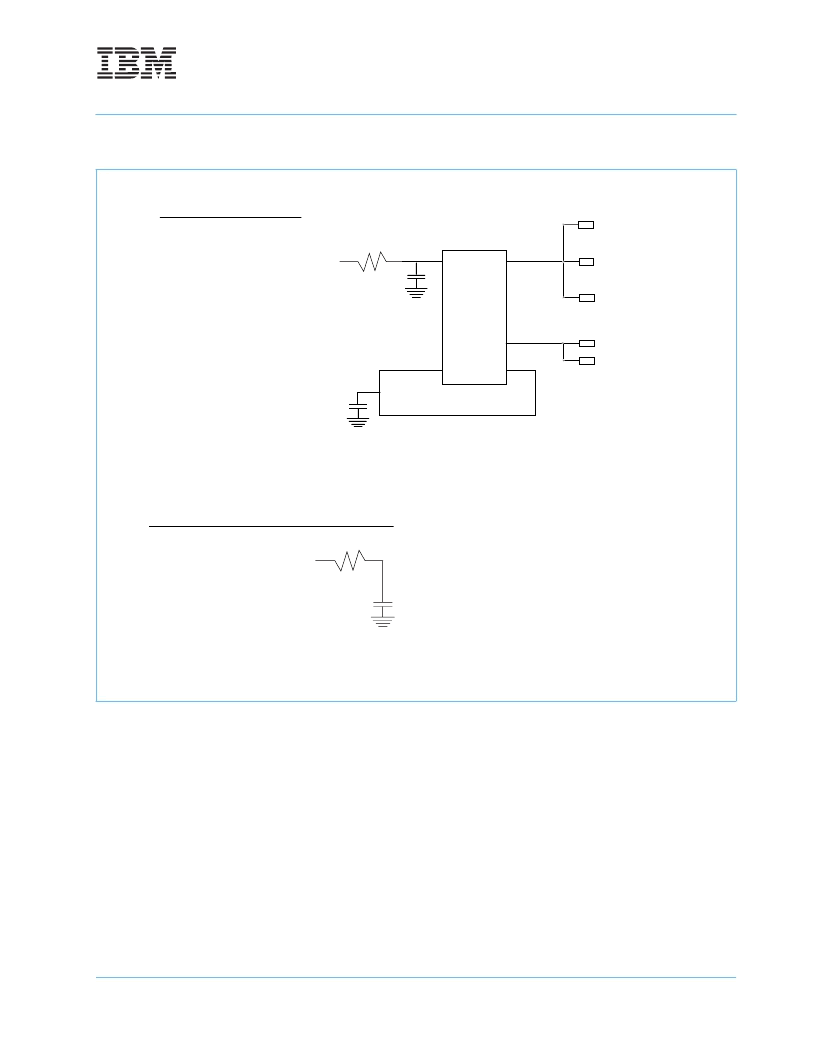
Clock Wiring
10 Ohms
CK0
Clock Net Wiring (CK0):
IN
SDRAM
SDRAM
All PLL clock SDRAM loads are equal--
achieved in part through equal-length
wiring.
FDBK
IN
(PLL out to Feedback input)
10 0hms
CK1, CK2, and CK3
Terminated Clock Nets (CK1, CK2, CK3):
PCK
OUT1
TO
OUT6
OUT10
12pF
Phase
Lock
Loop
1. The PLL is programmed via a combination of
the feedback path and on-DIMM loading.
PLL feedback produces zero phase shift
from the delayed CK0 input.
2. Card wiring and capacitance loading varia-
tion:
±
100 ps.
3. Timing is based on a driver with a 1 Volt/ns
rise time.
4. Feedback Capacitor Valve determined by
PLL phase characteristics.
Notes:
SDRAM
Register 1:1
Register 1:1
OUT7
PCK
One of six SDRAM outputs is shown.
12pF
12pF
相關(guān)PDF資料 |
PDF描述 |
|---|---|
| IBM13M64734BCA | 64M x 72 1 Bank Registered/Buffered SDRAM Module(64M x 72 1組寄存/緩沖同步動(dòng)態(tài)RAM模塊) |
| IBM13M64734CCA | 64M x 72 2-Bank Registered/Buffered SDRAM Module(64M x 72 2組寄存/緩沖同步動(dòng)態(tài)RAM模塊) |
| IBM13M64734HCA | 64M x 72 Two-Bank Registered SDRAM Module(64M x 72 2組帶寄存同步動(dòng)態(tài)RAM模塊) |
| IBM13M8734HCB | 8M x 72 1 Bank Registered SDRAM Module with PLL(8M x 72 1組帶鎖相環(huán)的寄存同步動(dòng)態(tài)RAM模塊) |
| IBM13M8734HCC | 8M x 72 1 Bank Registered/Buffered SDRAM Module(8M x 72 1組寄存/緩沖同步動(dòng)態(tài)RAM模塊) |
相關(guān)代理商/技術(shù)參數(shù) |
參數(shù)描述 |
|---|---|
| IBM14H5481 | 制造商:AVED Memory Products 功能描述: |
| IBM14H5540 | 制造商:AVED MEMORY PRODUCTS 功能描述: 制造商:AVED Memory Products 功能描述: |
| IBM17R8251 | 制造商:AVED Memory Products 功能描述: |
| IBM17R8252 | 制造商:AVED Memory Products 功能描述: |
| IBM1805T | 制造商:Schneider Electric 功能描述:IBM1805T |
發(fā)布緊急采購(gòu),3分鐘左右您將得到回復(fù)。