- 您現(xiàn)在的位置:買賣IC網(wǎng) > PDF目錄379205 > IBM13M8734HCB (IBM Microeletronics) 8M x 72 1 Bank Registered SDRAM Module with PLL(8M x 72 1組帶鎖相環(huán)的寄存同步動態(tài)RAM模塊) PDF資料下載
參數(shù)資料
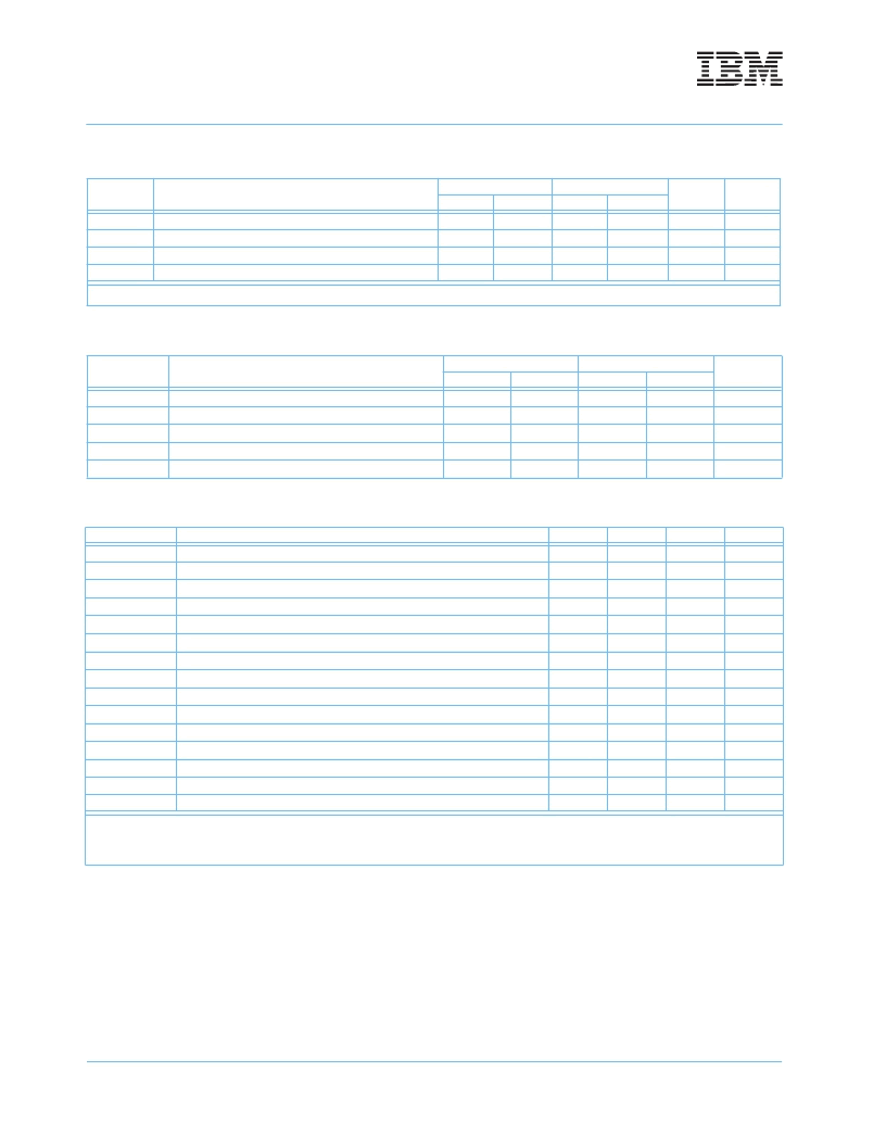
| 型號: | IBM13M8734HCB |
| 廠商: | IBM Microeletronics |
| 英文描述: | 8M x 72 1 Bank Registered SDRAM Module with PLL(8M x 72 1組帶鎖相環(huán)的寄存同步動態(tài)RAM模塊) |
| 中文描述: | 8米× 72 1帶鎖相環(huán)銀行注冊內(nèi)存模塊(8米× 72 1組帶鎖相環(huán)的寄存同步動態(tài)內(nèi)存模塊) |
| 文件頁數(shù): | 16/19頁 |
| 文件大小: | 325K |
| 代理商: | IBM13M8734HCB |
IBM13M8734HCB
8M x 72 1 Bank Registered SDRAM Module with PLL
Preliminary
IBM Corporation. All rights reserved.
Use is further subject to the provisions at the end of this document.
Page 16 of 19
08J0514.E24449
4/98
Functional Description and Timing Diagrams
Refer to IBM 168 Pin SDRAM Registered DIMM Functional Description and Timing Diagrams (Document
01L5868.E24564, Revised 1/98 for SDRAM operation).
Refer to the IBM Application Notes Serial Presence Detect on Memory DIMMsand SDRAM Presence Detect
Definitions for the Serial Presence Detect functional description and timings.
Read Cycle
Symbol
Parameter
-360, -365, -370
Min.
3.6
1.9
4.9
3
-10
Units
Notes
Max.
Min.
3.6
1.9
4.9
3
Max.
t
OH
t
LZ
t
HZ
t
DQZ
Data Out Hold Time
Data Out to Low Impedance Time
Data Out to High Impedance Time
DQM Data Out Disable Latency
ns
ns
ns
9.9
11.9
1
CLK
1. Referenced to the time at which the output achieves the open circuit condition, not to output voltage levels.
Write Cycle
Symbol
Parameter
-360, -365, -370
Min.
2.0
2.0
20
10
1
-10
Units
Max.
Min.
3.0
2.0
0
0
1
Max.
t
DS
t
DH
t
DPL2
t
DPL3
t
DQW
Data In Setup Time
Data In Hold Time
Data Input to Precharge
Data Input to Precharge
DQM Write Mask Latency
ns
ns
ns
ns
CLK
Presence Detect Read and Write Cycle
Symbol
f
SCL
T
I
t
AA
t
BUF
t
HD:STA
t
LOW
t
HIGH
t
SU:STA
t
HD:DAT
t
SU:DAT
t
r
t
f
t
SU:STO
t
DH
t
WR
Parameter
Min.
Max.
100
100
3.5
Units
kHz
ns
μ
s
μ
s
μ
s
μ
s
μ
s
μ
s
μ
s
ns
μ
s
ns
μ
s
ns
ms
Notes
SCL Clock Frequency
Noise Suppression Time Constant at SCL, SDA Inputs
SCL Low to SDA Data Out Valid
Time the Bus Must Be Free before a New Transmission Can Start
Start Condition Hold Time
Clock Low Period
Clock High Period
Start Condition Setup Time (for a Repeated Start Condition)
Data In Hold Time
Data In Setup Time
SDA and SCL Rise Time
SDA and SCL Fall Time
Stop Condition Setup Time
Data Out Hold Time
Write Cycle Time
0.3
4.7
4.0
4.7
4.0
4.7
0
250
1
300
4.7
300
15
1
1. The write cycle time (t
WR
) is the time from a valid stop condition of a write sequence to the end of the internal erase/program cycle.
During the write cycle, the bus interface circuits are disabled, SDA is allowed to remain high per the bus-level pull-up resistor, and
the device does not respond to its slave address.
相關PDF資料 |
PDF描述 |
|---|---|
| IBM13M8734HCC | 8M x 72 1 Bank Registered/Buffered SDRAM Module(8M x 72 1組寄存/緩沖同步動態(tài)RAM模塊) |
| IBM13M8734HCD | 8M x 72 1 Bank Registered/Buffered SDRAM Module(8M x 72 1組寄存/緩沖同步動態(tài)RAM模塊) |
| IBM13N16644HCB | 16M x 64 Two-Bank Unbuffered SDRAM Module(16M x 64 2組不帶緩沖同步動態(tài)RAM模塊) |
| IBM13N16734HCB | 16M x 72 Two-Bank Unbuffered SDRAM Module(16M x 72 2組不帶緩沖同步動態(tài)RAM模塊) |
| IBM13N16644HC | 16M x 64 2 Bank Unbuffered SDRAM Module(16M x 64 2組不帶緩沖同步動態(tài)RAM模塊) |
相關代理商/技術參數(shù) |
參數(shù)描述 |
|---|---|
| IBM14H5481 | 制造商:AVED Memory Products 功能描述: |
| IBM14H5540 | 制造商:AVED MEMORY PRODUCTS 功能描述: 制造商:AVED Memory Products 功能描述: |
| IBM17R8251 | 制造商:AVED Memory Products 功能描述: |
| IBM17R8252 | 制造商:AVED Memory Products 功能描述: |
| IBM1805T | 制造商:Schneider Electric 功能描述:IBM1805T |
發(fā)布緊急采購,3分鐘左右您將得到回復。