- 您現(xiàn)在的位置:買賣IC網(wǎng) > PDF目錄379205 > IBM13Q8734HCA (IBM Microeletronics) 8M x 72 Registered SDRAM Module(8M x 72 200腳寄存同步動(dòng)態(tài)RAM模塊) PDF資料下載
參數(shù)資料
| 型號(hào): | IBM13Q8734HCA |
| 廠商: | IBM Microeletronics |
| 英文描述: | 8M x 72 Registered SDRAM Module(8M x 72 200腳寄存同步動(dòng)態(tài)RAM模塊) |
| 中文描述: | 8米× 72注冊(cè)內(nèi)存模塊(8米× 72 200腳寄存同步動(dòng)態(tài)內(nèi)存模塊) |
| 文件頁數(shù): | 1/14頁 |
| 文件大?。?/td> | 243K |
| 代理商: | IBM13Q8734HCA |
IBM13Q8734HCA
8M x 72 Registered SDRAM Module
04K8916.C75645C
4/99
IBM Corporation. All rights reserved.
Use is further subject to the provisions at the end of this document.
Page 1 of 14
Features
200-Pin JEDEC Standard, Registered 8-Byte
Dual In-line Memory Module
8M x 72 Synchronous DRAM DIMM
Performance:
Inputs and outputs are LVTTL (3.3V) compatible
Single 3.3V to 3.6V Power Supply
Single Pulsed RAS interface
Fully Synchronous to positive Clock Edge
Data Mask control
Auto Refresh (CBR) and Self Refresh
Automatic and controlled Precharge Commands
Programmable Operation:
-SDRAM CAS Latency: 2
-Burst Type: Sequential or Interleave
-Burst Length: 2
-Operation: Burst Read and Write or Multiple
Burst Read with Single Write
Suspend Mode and Power Down Mode
12/9/2 Addressing (Row/Column/Bank)
4096 Refresh cycles distributed across 64ms
Parallel Presence Detect
Card size: 6.05" x 1.50" x 0.158"
Gold contacts
SDRAM
S
in TSOP Type II Package
Description
IBM13Q8734HCA is a registered 200-pin Synchro-
nous DRAM Dual In-line Memory Module (DIMM)
which is organized as a 8Mx72 high-speed memory
array. The DIMM uses nine x8 SDRAMs in 400mil
TSOP II packages. The DIMM achieves high speed
data transfer rates of up to 66MHz by employing a
prefetch/pipeline hybrid architecture that supports
the JEDEC 1N rule while allowing very low burst
power.
The DIMM is intended to comply with all non-
optional JEDEC standards set for the 200-pin regis-
tered SDRAM DIMMs.
All control and address signals are synchronized
with the positive edge of an externally supplied
clock. They are latched in an on-DIMM pipeline reg-
ister and presented to the SDRAMs on the following
clock.
Prior to any Access operation, the CAS latency,
burst type, burst length, and burst operation type
must be programmed into the DIMM by address
inputs A0-A13 using the Mode Register Set cycle.
The DIMM uses parallel presence detects imple-
mented according to the JEDEC standard.
All IBM 200-pin DIMMs provide a high performance,
flexible 8-byte interface in a 6.05” long high-perfor-
mance footprint. Related products include both EDO
DRAM and SDRAM unbuffered DIMMs in both non-
parity x64 and ECC-Optimized x72 configurations in
the 168 pin form factor.
CAS Latency = 2*
Clock Frequency
Clock Cycle
Clock Access Time
* SDRAM CAS latency = 2; DIMM CAS Latency = 3
-10
66
15
11.3
Units
MHz
ns
ns
f
CK
t
CK2
t
AC2
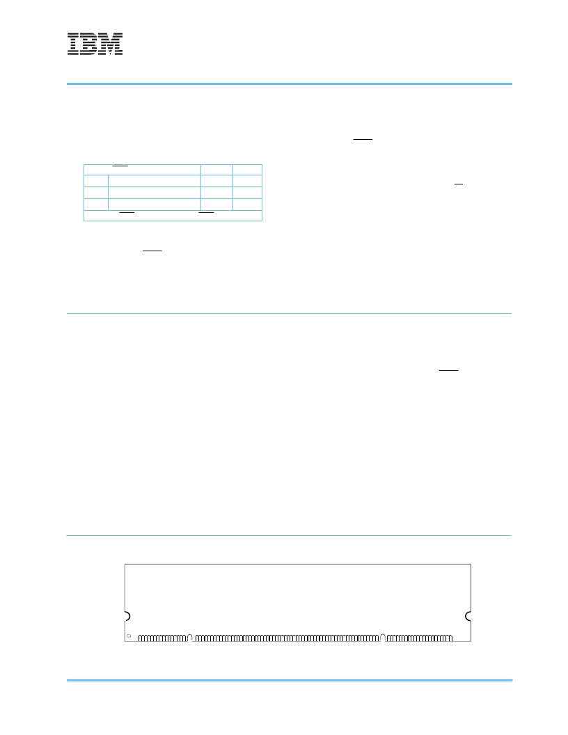
Card Outline
1
101
16
116
17
117
(Front)
(Back)
78
178
79
179
100
200
.
Discontinued (4/1/00 - last order; 7/31/00 - last ship)
相關(guān)PDF資料 |
PDF描述 |
|---|---|
| IBM13Q8739CC | 8M x 72 Registered SDRAM Module(帶寄存同步動(dòng)態(tài)RAM模塊(8M x 72高速存儲(chǔ)器陣列結(jié)構(gòu))) |
| IBM13T16644NPA | 16M x 64 PC100 SDRAM(1MB PC100 同步動(dòng)態(tài)RAM) |
| IBM13T2649JC | 2M x 64 SDRAM SO DIMM(Small Outline Dual In-Line Memory Module)(2M x 64 小外形雙列直插同步動(dòng)態(tài)RAM模塊) |
| IBM13T2649NC | 2M x 64 SDRAM SO DIMM(2M x 64小外形雙列直插同步動(dòng)態(tài)RAM模塊) |
| IBM13T4644MC | 1M x 64 SDRAM SO DIMM(1M x 64 同步動(dòng)態(tài)RAM模塊) |
相關(guān)代理商/技術(shù)參數(shù) |
參數(shù)描述 |
|---|---|
| IBM14H5481 | 制造商:AVED Memory Products 功能描述: |
| IBM14H5540 | 制造商:AVED MEMORY PRODUCTS 功能描述: 制造商:AVED Memory Products 功能描述: |
| IBM17R8251 | 制造商:AVED Memory Products 功能描述: |
| IBM17R8252 | 制造商:AVED Memory Products 功能描述: |
| IBM1805T | 制造商:Schneider Electric 功能描述:IBM1805T |
發(fā)布緊急采購(gòu),3分鐘左右您將得到回復(fù)。