- 您現(xiàn)在的位置:買賣IC網(wǎng) > PDF目錄379205 > IBM13Q8739CC (IBM Microeletronics) 8M x 72 Registered SDRAM Module(帶寄存同步動態(tài)RAM模塊(8M x 72高速存儲器陣列結(jié)構(gòu))) PDF資料下載
參數(shù)資料
| 型號: | IBM13Q8739CC |
| 廠商: | IBM Microeletronics |
| 英文描述: | 8M x 72 Registered SDRAM Module(帶寄存同步動態(tài)RAM模塊(8M x 72高速存儲器陣列結(jié)構(gòu))) |
| 中文描述: | 8米× 72注冊內(nèi)存模塊(帶寄存同步動態(tài)內(nèi)存模塊(8米× 72高速存儲器陣列結(jié)構(gòu))) |
| 文件頁數(shù): | 26/56頁 |
| 文件大小: | 903K |
| 代理商: | IBM13Q8739CC |
第1頁第2頁第3頁第4頁第5頁第6頁第7頁第8頁第9頁第10頁第11頁第12頁第13頁第14頁第15頁第16頁第17頁第18頁第19頁第20頁第21頁第22頁第23頁第24頁第25頁當前第26頁第27頁第28頁第29頁第30頁第31頁第32頁第33頁第34頁第35頁第36頁第37頁第38頁第39頁第40頁第41頁第42頁第43頁第44頁第45頁第46頁第47頁第48頁第49頁第50頁第51頁第52頁第53頁第54頁第55頁第56頁
IBM13Q8739CC
8M x 72 Registered SDRAM Module
IBM Corporation. All rights reserved.
Use is further subject to the provisions at the end of this document.
Page 26 of 56
08J0513.E24526
Revised 4/98
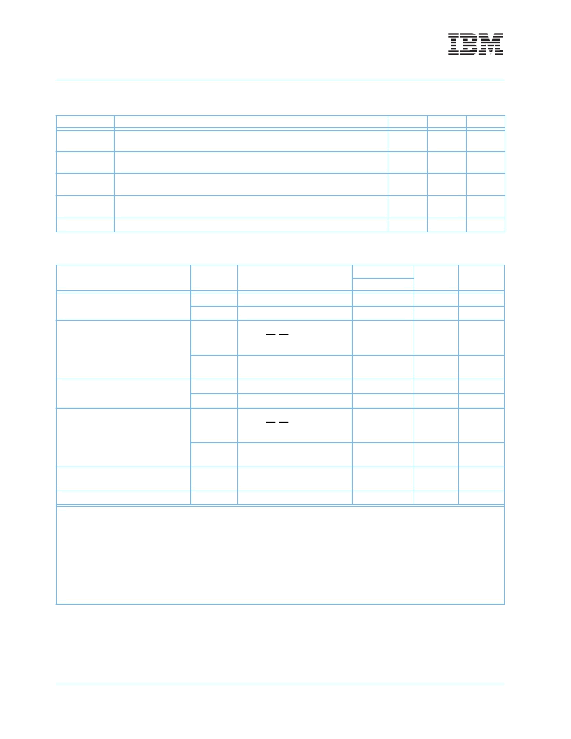
Output Characteristics
(T
A
= 0 to +70C, V
DD
= 3.3V to 3.6V)
Symbol
Parameter
Min.
Max.
Units
I
I(L)
Input Leakage Current, any input
(0.0V
≤
V
IN
≤
3.6V), All Other Pins Not Under Test = 0V
-10
+10
μ
A
I
O(L)
Output Leakage Current (DQ)
(D
OUT
is disabled, 0.0V
≤
V
OUT
≤
3.6V)
-2
+2
μ
A
V
OH
Output Level (TTL)
Output “H” Level Voltage (I
OUT
= -2.0mA)
2.4
V
DD
V
V
OL
Output Level (TTL)
Output “L” Level Voltage (I
OUT
= +2.0mA)
0.0
0.4
V
I
O(L)
Output Leakage Current (PD1 - PD8)
-10
+10
μ
A
Standby and Refresh Currents
(T
A
= 0 to +70C, V
DD
= 3.3V to 3.6V)
Parameter
Symbol
Test Condition
Organization
Units
Notes
x72
Precharge Standby Current in Power
Down Mode
I
CC1
P
CKE0
≤
V
IL
(max), t
CK
= 15ns
364
mA
1
I
CC1
PS
CKE0
≤
V
IL
(max), t
CK
= Infinity
75
mA
1
Precharge Standby Current in Non-
Power Down Mode
I
CC1
N
CKE0
≥
V
IH
(min), t
CK
= 15ns,
S0, S1
≥
V
IH
(min)
Input Change every 30ns
1200
mA
1
I
CC1
NS
CKE0
≥
V
IH
(min), t
CK
= Infinity
No Input Change
363
mA
1
Active Standby Current in Power Down
Mode
I
CC2
P
CKE0
≤
V
IL
(max), t
CK
= 15ns
364
mA
1, 2
I
CC2
PS
CKE0
≤
V
IL
(max), t
CK
= Infinity
75
mA
1, 2
Active Standby Current in Non-Power
Down Mode
I
CC2
N
CKE0
≥
V
IH
(min), t
CK
= 15ns,
S0, S1
≥
V
IH
(min)
Input Change every 30ns
1200
mA
3
I
CC2
NS
CKE0
≥
V
IH
(min), t
CK
= Infinity
No Input Change
453
mA
4
Auto (CBR) Refresh Current
I
CC3
CAS Latency = 2
t
RC
≥
t
RC
(min)
2370
mA
5, 6, 7, 8
Self Refresh Current
I
CC4
CKE0
≤
0.2V
326
mA
1
1. The specified values are for both DIMM banks operating in the specified mode.
2. Active Standby Current will be higher if Clock Suspend is entered during a Burst Read cycle (add 1mA per DQ).
3. The specified values are for one DIMM bank in Active Standby and the other DIMM bank in Precharge Standby (I
CC2
N and I
CC1
N).
4. The specified values are for one DIMM bank in Active Standby and the other DIMM bank in Precharge Standby (I
CC2
NS and
I
CC1
NS).
5. The specified values are valid when addresses are changed no more than once during t
CK
(min).
6. The specified values are valid when No operation commands are registered on every rising clock edge during t
RC
(min).
7. The specified values are valid when data inputs (DQs) are stable during t
RC
(min).
8. The specified values are for one DIMM bank in Auto Refresh (CBR) and the other DIMM bank in Precharge Standby (I
CC1
N).
相關(guān)PDF資料 |
PDF描述 |
|---|---|
| IBM13T16644NPA | 16M x 64 PC100 SDRAM(1MB PC100 同步動態(tài)RAM) |
| IBM13T2649JC | 2M x 64 SDRAM SO DIMM(Small Outline Dual In-Line Memory Module)(2M x 64 小外形雙列直插同步動態(tài)RAM模塊) |
| IBM13T2649NC | 2M x 64 SDRAM SO DIMM(2M x 64小外形雙列直插同步動態(tài)RAM模塊) |
| IBM13T4644MC | 1M x 64 SDRAM SO DIMM(1M x 64 同步動態(tài)RAM模塊) |
| IBM13T1649NC | 1M x 64 SDRAM SO DIMM(1M x 64 同步動態(tài)RAM模塊) |
相關(guān)代理商/技術(shù)參數(shù) |
參數(shù)描述 |
|---|---|
| IBM14H5481 | 制造商:AVED Memory Products 功能描述: |
| IBM14H5540 | 制造商:AVED MEMORY PRODUCTS 功能描述: 制造商:AVED Memory Products 功能描述: |
| IBM17R8251 | 制造商:AVED Memory Products 功能描述: |
| IBM17R8252 | 制造商:AVED Memory Products 功能描述: |
| IBM1805T | 制造商:Schneider Electric 功能描述:IBM1805T |
發(fā)布緊急采購,3分鐘左右您將得到回復(fù)。