- 您現在的位置:買賣IC網 > PDF目錄379205 > IBM13T2649JC (IBM Microeletronics) 2M x 64 SDRAM SO DIMM(Small Outline Dual In-Line Memory Module)(2M x 64 小外形雙列直插同步動態(tài)RAM模塊) PDF資料下載
參數資料
| 型號: | IBM13T2649JC |
| 廠商: | IBM Microeletronics |
| 英文描述: | 2M x 64 SDRAM SO DIMM(Small Outline Dual In-Line Memory Module)(2M x 64 小外形雙列直插同步動態(tài)RAM模塊) |
| 中文描述: | 200萬蘇× 64 SDRAM的內存(小外形雙列內存模組)(2米× 64小外形雙列直插同步動態(tài)內存模塊) |
| 文件頁數: | 4/15頁 |
| 文件大小: | 299K |
| 代理商: | IBM13T2649JC |
IBM13T2649JC
2M x 64 SDRAM SO DIMM
IBM Corporation. All rights reserved.
Use is further subject to the provisions at the end of this document.
Page 4 of 15
75H5376
GA14-4476-02
Rev 3/98
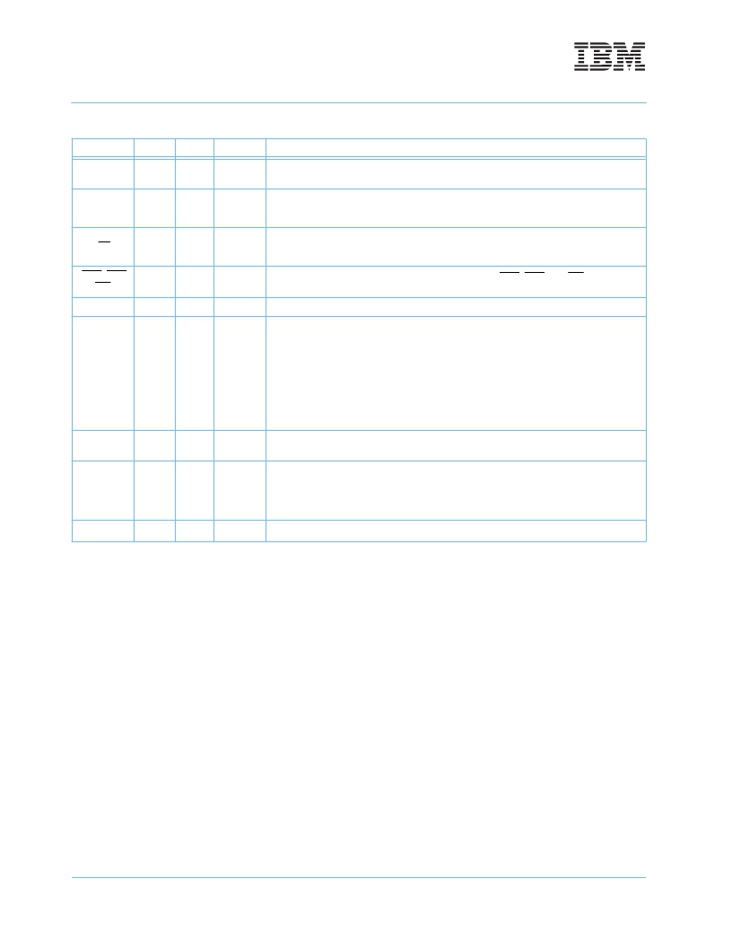
Input/Output Functional Description
Symbol
Type
Signal
Polarity
Function
CK0, CK1
Input
Pulse
Positive
Edge
The system clock inputs. All of the SDRAM inputs are sampled on the rising edge of their
associated clock.
CKE0
Input
Level
Active
High
Activates the CK0 and CK1 signals when high and deactivates them when low. By deac-
tivating the clocks, CKE0 low initiates the Power Down mode, Suspend mode, or the Self
Refresh mode.
S0
Input
Pulse
Active Low
Enables the associated SDRAM command decoder when low and disables the command
decoder when high. When the command decoder is disabled, new commands are
ignored but previous operations continue.
RAS, CAS
WE
Input
Pulse
Active Lowoperation to be executed by the SDRAM.
BA0
Input
Level
—
Selects which SDRAM bank is to be active.
A0 - A9
A10/AP
Input
Level
—
During a Bank Activate command cycle, A0-A10 defines the row address (RA0-RA10)
when sampled at the rising clock edge.
During a Read or Write command cycle, A0-A8 defines the column address (CA0-CA8)
when sampled at the rising clock edge. In addition to the column address, AP is used to
invoke autoprecharge operation at the end of the burst read or write cycle. If AP is high,
autoprecharge is selected and BA0 defines the bank to be precharged (low=bank A,
high=bank B). If AP is low, autoprecharge is disabled.
During a Precharge command cycle, AP is used in conjunction with BA0 to control which
bank(s) to precharge. If AP is high, both bank A and bank B will be precharged regard-
less of the state of BA0. If AP is low, then BA0 is used to define which bank to precharge.
DQ0 - DQ63
Input
Output
Level
—
Data Input/Output pins operate in the same manner as on conventional DRAMs.
DQMB0 -
DQMB7
Input
Pulse
Active
High
The Data Input/Output mask places the DQ buffers in a high impedance state when sam-
pled high. In Read mode, DQM has a latency of two clock cycles and controls the output
buffers like an output enable. In Write mode, DQM has a latency of zero and operates as
a byte mask by allowing input data to be written if it is low but blocks the write operation if
DQM is high.
VDD, VSS
Supply
Power and ground for the module.
Discontinued (12/98 - last order; 9/99 last ship)
相關PDF資料 |
PDF描述 |
|---|---|
| IBM13T2649NC | 2M x 64 SDRAM SO DIMM(2M x 64小外形雙列直插同步動態(tài)RAM模塊) |
| IBM13T4644MC | 1M x 64 SDRAM SO DIMM(1M x 64 同步動態(tài)RAM模塊) |
| IBM13T1649NC | 1M x 64 SDRAM SO DIMM(1M x 64 同步動態(tài)RAM模塊) |
| IBM13T4644MPC | 4M x 64 SDRAM SO DIMM(Small Outline Dual In-line Memory Module)(4M x 64小外形雙列直插同步動態(tài)RAM模塊) |
| IBM13T4644MPD | One Bank 4M x 64 SDRAM SO DIMM(Small Outline Dual In-line Memory Module)(1組 4M x 64 PC100小外形雙列直插同步動態(tài)RAM模塊) |
相關代理商/技術參數 |
參數描述 |
|---|---|
| IBM14H5481 | 制造商:AVED Memory Products 功能描述: |
| IBM14H5540 | 制造商:AVED MEMORY PRODUCTS 功能描述: 制造商:AVED Memory Products 功能描述: |
| IBM17R8251 | 制造商:AVED Memory Products 功能描述: |
| IBM17R8252 | 制造商:AVED Memory Products 功能描述: |
| IBM1805T | 制造商:Schneider Electric 功能描述:IBM1805T |
發(fā)布緊急采購,3分鐘左右您將得到回復。