- 您現(xiàn)在的位置:買(mǎi)賣(mài)IC網(wǎng) > PDF目錄379206 > IBMB6M32734HGA (IBM Microeletronics) 32M x72 One Bank Registered DDR SDRAM Module(32M x 72 1組寄存同步雙數(shù)據(jù)速率動(dòng)態(tài)RAM模塊) PDF資料下載
參數(shù)資料
| 型號(hào): | IBMB6M32734HGA |
| 廠商: | IBM Microeletronics |
| 英文描述: | 32M x72 One Bank Registered DDR SDRAM Module(32M x 72 1組寄存同步雙數(shù)據(jù)速率動(dòng)態(tài)RAM模塊) |
| 中文描述: | 32M的x72第一銀行注冊(cè)DDR SDRAM內(nèi)存模塊(32M × 72配置一組寄存同步雙數(shù)據(jù)速率動(dòng)態(tài)內(nèi)存模塊) |
| 文件頁(yè)數(shù): | 5/23頁(yè) |
| 文件大小: | 421K |
| 代理商: | IBMB6M32734HGA |
第1頁(yè)第2頁(yè)第3頁(yè)第4頁(yè)當(dāng)前第5頁(yè)第6頁(yè)第7頁(yè)第8頁(yè)第9頁(yè)第10頁(yè)第11頁(yè)第12頁(yè)第13頁(yè)第14頁(yè)第15頁(yè)第16頁(yè)第17頁(yè)第18頁(yè)第19頁(yè)第20頁(yè)第21頁(yè)第22頁(yè)第23頁(yè)
IBMB6M32734HGA
Preliminary
32Mx72 One Bank Registered DDR SDRAM Module
19L7358.H02502A
1/01
IBM Corporation. All rights reserved.
Use is further subject to the provisions at the end of this document.
Page 5 of 23
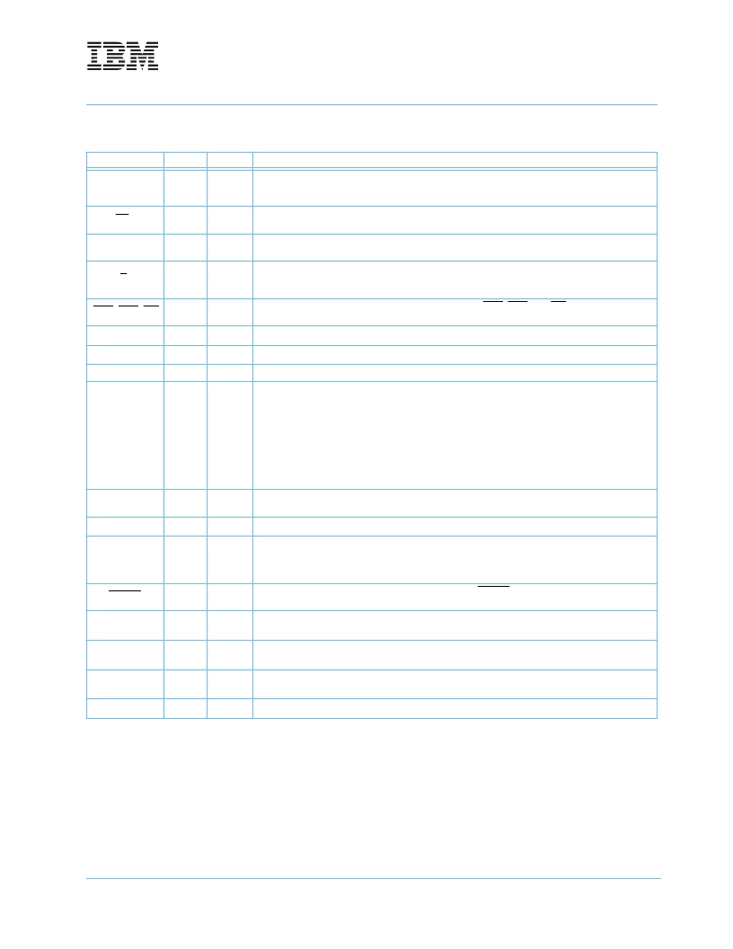
Input/Output Functional Description
Symbol
Type
Polarity
Function
CK0
(SSTL)
Positive
Edge
The positive line of the differential pair of system clock inputs which drives the input to the on-
DIMM PLL. All the DDR SDRAM address and control inputs are sampled on the rising edge of
their associated clocks.
CK0
(SSTL)
Negative
Edge
The negative line of the differential pair of system clock inputs which drives the input to the on-
DIMM PLL.
CKE0
(SSTL)
Active
High
Activates the SDRAM CK signal when high and deactivates the CK signal when low. By deacti-
vating the clocks, CKE low initiates the Power Down mode, or the Self Refresh mode.
S0
(SSTL)
Active
Low
Enables the associated SDRAM command decoder when low and disables the command
decoder when high. When the command decoder is disabled, new commands are ignored but
previous operations continue.
RAS, CAS, WE
(SSTL)
Active
Low
When sampled at the positive rising edge of the clock, CAS, RAS, and WE define the operation
to be executed by the SDRAM.
V
REF
Supply
Reference voltage for SSTL-2 inputs
V
DDQ
Supply
Isolated power supply for the DDR SDRAM output buffers to provide improved noise immunity
BA0,1
(SSTL)
—
Selects which SDRAM bank of four is activated.
A0 - A9, A11,
A12, A10/AP
(SSTL)
—
During a Bank Activate command cycle, A0-A12 defines the row address (RA0-RA12) when
sampled at the rising clock edge.
During a Read or Write command cycle, A0-A9 defines the column address (CA0-CA9) when
sampled at the rising clock edge. In addition to the column address, AP is used to invoke auto-
precharge operation at the end of the burst read or write cycle. If AP is high, autoprecharge is
selected and BA0, BA1 defines the bank to be precharged. If AP is low, autoprecharge is dis-
abled.
During a Precharge command cycle, AP is used in conjunction with BA0, BA1 to control which
bank(s) to precharge. If AP is high, all banks will be precharged regardless of the state of BA0
or BA1. If AP is low, BA0 and BA1 are used to define which bank to precharge.
DQ0 - DQ63,
CB0 - CB7
(SSTL)
—
Data and Check Bit Input/Output pins. Check bits are only applicable on the x72 DIMM config-
urations.
V
DD
, V
SS
Supply
Power and ground for the DDR SDRAM input buffers and core logic
DQS0-DQS17
(SSTL)
Negative
and
Positive
Edge
Data strobe for input and output data
RESET
(LVC-
MOS)
Active
Low
Asynchronously forces all register outputs low when RESET is low. This signal can be used
during power up to ensure CKE0 and CKE1 are low and SDRAM DQSs are Hi-Z.
SA0 - 2
—
These signals are tied at the system planar to either V
SS
or V
DD
to configure the serial SPD
EEPROM address range.
SDA
—
This bidirectional pin is used to transfer data into or out of the SPD EEPROM. A resistor must
be connected from the SDA bus line to V
DD
to act as a pullup.
SCL
—
This signal is used to clock data into and out of the SPD EEPROM. A resistor may be con-
nected from the SCL bus time to V
DD
to act as a pullup.
V
DDSPD
Supply
Serial EEPROM positive power supply.
相關(guān)PDF資料 |
PDF描述 |
|---|---|
| IBMN312404CT3 | 128Mb(2Mbit x 16 I/O x 4 Bank) Synchronous DRAM(128M位(2M位 x 16 I/O x 4 組)同步動(dòng)態(tài)RAM) |
| IBMN312804CT3 | 128Mb(4Mbit x 8 I/O x 4 Bank) Synchronous DRAM(128M位(4M位 x 8 I/O x 4 組)同步動(dòng)態(tài)RAM) |
| IBMN312164CT3 | 128Mb(8Mbit x 4 I/O x 4 Bank) Synchronous DRAM(128M位(8M位 x 4 I/O x 4 組)同步動(dòng)態(tài)RAM) |
| IBMN325404CT3 | 256Mb(4Mbit x 16 I/O x 4 Bank) Synchronous DRAM(256M位(4M位 x 16 I/O x 4 組)同步動(dòng)態(tài)RAM) |
| IBMN325804CT3 | 256Mb(8Mbit x 8 I/O x 4 Bank) Synchronous DRAM(256M位(8M位 x 8 I/O x 4 組)同步動(dòng)態(tài)RAM) |
相關(guān)代理商/技術(shù)參數(shù) |
參數(shù)描述 |
|---|---|
| IBMFDM44H-064J | 制造商:STEC Inc 功能描述:64MB FLASH 44PIN HORIZ IBM - Bulk |
| IBMFDM44H-064J-01 | 制造商:STEC Inc 功能描述:AKA:IBM00-01234-0A1C - Bulk |
| IBMFDM44H-064JU-01 | 制造商:STEC Inc 功能描述:AKA: IBM00-01234-0B1CU - Bulk |
| IBMFDM44H-128MM1U | 制造商:STEC Inc 功能描述:128MB CF, COMMERCIAL TEMP - Bulk |
| IBMN364164CT3C360 | 制造商:IBM 功能描述:* |
發(fā)布緊急采購(gòu),3分鐘左右您將得到回復(fù)。