- 您現(xiàn)在的位置:買賣IC網(wǎng) > PDF目錄362808 > IC42S16102-7BG 512K x 16 Bit x 2 Banks (16-MBIT) SDRAM PDF資料下載
參數(shù)資料
| 型號(hào): | IC42S16102-7BG |
| 英文描述: | 512K x 16 Bit x 2 Banks (16-MBIT) SDRAM |
| 中文描述: | 為512k × 16位× 2銀行(16兆)內(nèi)存 |
| 文件頁(yè)數(shù): | 35/78頁(yè) |
| 文件大?。?/td> | 790K |
| 代理商: | IC42S16102-7BG |
第1頁(yè)第2頁(yè)第3頁(yè)第4頁(yè)第5頁(yè)第6頁(yè)第7頁(yè)第8頁(yè)第9頁(yè)第10頁(yè)第11頁(yè)第12頁(yè)第13頁(yè)第14頁(yè)第15頁(yè)第16頁(yè)第17頁(yè)第18頁(yè)第19頁(yè)第20頁(yè)第21頁(yè)第22頁(yè)第23頁(yè)第24頁(yè)第25頁(yè)第26頁(yè)第27頁(yè)第28頁(yè)第29頁(yè)第30頁(yè)第31頁(yè)第32頁(yè)第33頁(yè)第34頁(yè)當(dāng)前第35頁(yè)第36頁(yè)第37頁(yè)第38頁(yè)第39頁(yè)第40頁(yè)第41頁(yè)第42頁(yè)第43頁(yè)第44頁(yè)第45頁(yè)第46頁(yè)第47頁(yè)第48頁(yè)第49頁(yè)第50頁(yè)第51頁(yè)第52頁(yè)第53頁(yè)第54頁(yè)第55頁(yè)第56頁(yè)第57頁(yè)第58頁(yè)第59頁(yè)第60頁(yè)第61頁(yè)第62頁(yè)第63頁(yè)第64頁(yè)第65頁(yè)第66頁(yè)第67頁(yè)第68頁(yè)第69頁(yè)第70頁(yè)第71頁(yè)第72頁(yè)第73頁(yè)第74頁(yè)第75頁(yè)第76頁(yè)第77頁(yè)第78頁(yè)
IC42S16102
Integrated Circuit Solution Inc.
DR042-0A 01/18/2005
35
CAS
latency = 2, burst length = 4
READ 0
COMMAND
CKE
I/O
CLK
D
OUT
0
D
OUT
1
D
OUT
2
D
OUT
3
READ (BANK 0)
CLOCK SUSPEND
Bank Active Command Interval
When the selected bank is precharged, the period trp has
elapsed and the bank has entered the idle state, the bank
can be activated by executing the active command. If the
other bank is in the idle state at that time, the active
command can be executed for that bank after the period
t
RRD
has elapsed. At that point both banks will be in the
active state. When a bank active command has been
executed, a precharge command must be executed for
that bank within the ACT to PRE command period (t
RAS
max). Also note that a precharge command cannot be
executed for an active bank before t
RAS
(min) has elapsed.
After a bank active command has been executed and the
trcd period has elapsed, read write (including auto-
precharge) commands can be executed for that bank.
ACT 0
ACT 1
COMMAND
CLK
BANK ACTIVE (BANK 0)
BANK ACTIVE (BANK 1)
t
RRD
ACT 0
READ 0
COMMAND
CLK
BANK ACTIVE (BANK 0)
BANK ACTIVE (BANK 0)
t
RCD
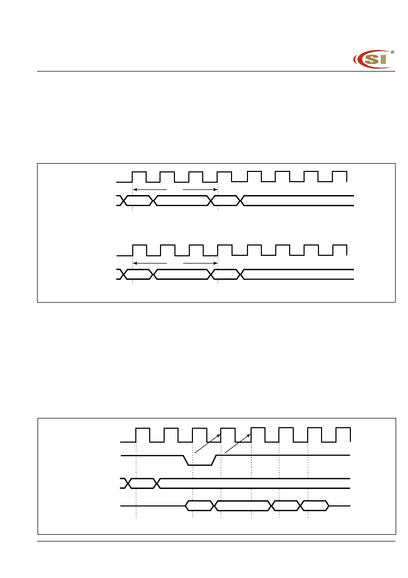
Clock Suspend
When the CKE pin is dropped from HIGH to LOW during
a read or write cycle, the IS42S16102 enters clock
suspend mode on the next CLK rising edge. This command
reduces the device power dissipation by stopping the
device internal clock. Clock suspend mode continues as
long as the CKE pin remains low. In this state, all inputs
other than CKE pin are invalid and no other commands
can be executed. Also, the device internal states are
maintained. When the CKE pin goes from LOW to HIGH
clock suspend mode is terminated on the next CLK rising
edge and device operation resumes.
The next command cannot be executed until the recovery
period (t
CKA
) has elapsed.
Since this command differs from the self-refresh command
described previously in that the refresh operation is not
performed automatically internally, the refresh operation
must be performed within the refresh period (tref). Thus
the maximum time that clock suspend mode can be held
is just under the refresh cycle time.
CAS
latency = 3
相關(guān)PDF資料 |
PDF描述 |
|---|---|
| IC42S16102-7BIG | 512K x 16 Bit x 2 Banks (16-MBIT) SDRAM |
| IC42S16102-7T | 512K x 16 Bit x 2 Banks (16-MBIT) SDRAM |
| IC42S16102-7TG | 512K x 16 Bit x 2 Banks (16-MBIT) SDRAM |
| IC42S16102-7TI | 512K x 16 Bit x 2 Banks (16-MBIT) SDRAM |
| IC42S16102-7TIG | 512K x 16 Bit x 2 Banks (16-MBIT) SDRAM |
相關(guān)代理商/技術(shù)參數(shù) |
參數(shù)描述 |
|---|---|
| IC42S16102-7BIG | 制造商:ICSI 制造商全稱:Integrated Circuit Solution Inc 功能描述:512K x 16 Bit x 2 Banks (16-MBIT) SDRAM |
| IC42S16102-7T | 制造商:ICSI 制造商全稱:Integrated Circuit Solution Inc 功能描述:512K x 16 Bit x 2 Banks (16-MBIT) SDRAM |
| IC42S16102-7TG | 制造商:ICSI 制造商全稱:Integrated Circuit Solution Inc 功能描述:512K x 16 Bit x 2 Banks (16-MBIT) SDRAM |
| IC42S16102-7TI | 制造商:ICSI 制造商全稱:Integrated Circuit Solution Inc 功能描述:512K x 16 Bit x 2 Banks (16-MBIT) SDRAM |
| IC42S16102-7TIG | 制造商:ICSI 制造商全稱:Integrated Circuit Solution Inc 功能描述:512K x 16 Bit x 2 Banks (16-MBIT) SDRAM |
發(fā)布緊急采購(gòu),3分鐘左右您將得到回復(fù)。