- 您現(xiàn)在的位置:買賣IC網(wǎng) > PDF目錄362808 > IC43R16160-5T 4M x 16 Bit x 4 Banks (256-MBIT) DDR SDRAM PDF資料下載
參數(shù)資料
| 型號: | IC43R16160-5T |
| 英文描述: | 4M x 16 Bit x 4 Banks (256-MBIT) DDR SDRAM |
| 中文描述: | 4米× 16位× 4個銀行(256兆)DDR SDRAM內(nèi)存 |
| 文件頁數(shù): | 31/56頁 |
| 文件大小: | 1271K |
| 代理商: | IC43R16160-5T |
第1頁第2頁第3頁第4頁第5頁第6頁第7頁第8頁第9頁第10頁第11頁第12頁第13頁第14頁第15頁第16頁第17頁第18頁第19頁第20頁第21頁第22頁第23頁第24頁第25頁第26頁第27頁第28頁第29頁第30頁當(dāng)前第31頁第32頁第33頁第34頁第35頁第36頁第37頁第38頁第39頁第40頁第41頁第42頁第43頁第44頁第45頁第46頁第47頁第48頁第49頁第50頁第51頁第52頁第53頁第54頁第55頁第56頁
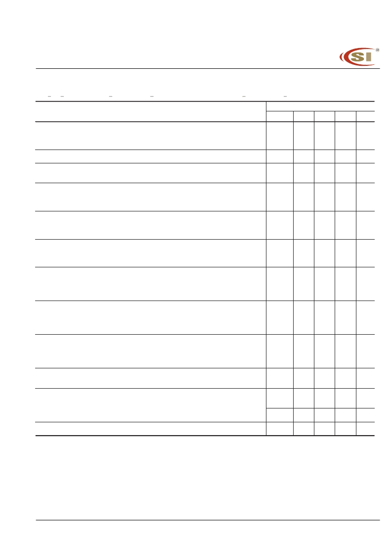
IDD Max Specifications and Conditions
(0°C < TA < 70°C, VDDQ=2.5V+ 0.2V, VDD=2.5 +0.2V, for DDR400 device VDDQ=2.6V+ 0.1V, VDD=2.6 +0.1V
Symbol
-5
-6
-7
Unit
Operating current - One bank Active-Precharge;
tRC=tRCmin;tCK=133Mhz for
DDR266, 166Mhz for DDR333; DQ,DM and DQS inputs chang-ing twice per clock
cycle; address and control inputs changing once per clock cycle
IDD0
120
110
100
mA
Operating current - One bank operation;
One bank open, BL=4
IDD1
160
140
120
mA
Percharge power-down standby current; All banks idle;
power - down mode; CKE
=< VIL(max); tCK=133Mhz for DDR266; Vin = Vref for DQ,DQS and DM
IDD2P
30
25
20
mA
Precharge Floating standby current;
CS# > =VIH(min);All banks idle; CKE > =
VIH(min); tCK=133Mhz for DDR266; Address and other control inputs changing once
per clock cycle; Vin = Vref for DQ,DQS and DM
IDD2F
52
45
38
mA
Precharge Quiet standby current;
CS# > = VIH(min); All banks idle; CKE > =
VIH(min); tCK =133Mhz for DDR266; Address and other control inputs stable with
keeping >= VIH(min) or =<VIL(max); Vin = Vref for DQ ,DQS and DM
IDD2Q
50
44
37
mA
Active power - down standby current;
one bank active; power-down mode; CKE=<
VIL (max); tCK =133Mhz for DDR266, 166MHZ for DDR333; Vin = Vref for DQ,DQS
and DM
IDD3P
30
25
20
mA
Active standby current;
CS# >= VIH(min); CKE>=VIH(min); one bank active; active -
precharge; tRC=tRASmax; tCK =133Mhz for DDR266, 166Mhz for DDR333; DQ, DQS
and DM inputs changing twice per clock cycle; address and other control inputs
changing once per clock cycle
IDD3N
90
80
70
mA
Operating current - burst read;
Burst length = 2; reads; continguous burst; One bank
active; address and control inputs changing once per clock cycle; CL=2 at tCK =
133Mhz for DDR266, CL=2.5 at tCK=166Mhz for DDR333; 50% of data changing at
every burst; lout = 0 m A
IDD4R
270
230
190
mA
Operating current - burst write;
Burst length = 2; writes; continuous burst; One bank
active address and control inputs changing once per clock cycle; CL=2 at tCK =
133Mhz for DDR266 ; DQ, DM and DQS inputs changing twice per clock cycle, 50% of
input data changing at every burst
IDD4W
250
210
170
mA
Auto refresh current;
tRC = tRFC(min) - 10*tCK for DDR266 at 133Mhz, 12*tCK for
DDR333; distributed refresh
IDD5
210
200
190
mA
Self refresh current;
CKE =< 0.2V; External clock should be on; tCK =133Mhz for
DDR266, 166Mhz for DDR333.
IDD6
(nomal)
3
3
3
mA
Self refresh current;
(Low Power)
(L)
1.8
1.8
1.8
mA
Operating current - Four bank operation;
Four bank interleaving with BL=4
IDD7
400
350
300
mA
Conditions
Version
IC4
3R16160
Integrated Circuit Solution Inc.
DDR001-0B
1
1
/
10
/
2004
31
相關(guān)PDF資料 |
PDF描述 |
|---|---|
| IC43R16160-5TG | 4M x 16 Bit x 4 Banks (256-MBIT) DDR SDRAM |
| IC43R16160-6T | 4M x 16 Bit x 4 Banks (256-MBIT) DDR SDRAM |
| IC43R16160-6TG | 4M x 16 Bit x 4 Banks (256-MBIT) DDR SDRAM |
| IC43R16160-7T | 4M x 16 Bit x 4 Banks (256-MBIT) DDR SDRAM |
| IC43R16160-7TG | 4M x 16 Bit x 4 Banks (256-MBIT) DDR SDRAM |
相關(guān)代理商/技術(shù)參數(shù) |
參數(shù)描述 |
|---|---|
| IC43R16160-5TG | 制造商:ICSI 制造商全稱:Integrated Circuit Solution Inc 功能描述:4M x 16 Bit x 4 Banks (256-MBIT) DDR SDRAM |
| IC43R16160-6T | 制造商:ICSI 制造商全稱:Integrated Circuit Solution Inc 功能描述:4M x 16 Bit x 4 Banks (256-MBIT) DDR SDRAM |
| IC43R16160-6TG | 制造商:ICSI 制造商全稱:Integrated Circuit Solution Inc 功能描述:4M x 16 Bit x 4 Banks (256-MBIT) DDR SDRAM |
| IC43R16160-7T | 制造商:ICSI 制造商全稱:Integrated Circuit Solution Inc 功能描述:4M x 16 Bit x 4 Banks (256-MBIT) DDR SDRAM |
| IC43R16160-7TG | 制造商:ICSI 制造商全稱:Integrated Circuit Solution Inc 功能描述:4M x 16 Bit x 4 Banks (256-MBIT) DDR SDRAM |
發(fā)布緊急采購,3分鐘左右您將得到回復(fù)。