- 您現(xiàn)在的位置:買賣IC網(wǎng) > PDF目錄61089 > IDTCSP59920-5SO (INTEGRATED DEVICE TECHNOLOGY INC) PLL BASED CLOCK DRIVER, 8 TRUE OUTPUT(S), 0 INVERTED OUTPUT(S), PDSO24 PDF資料下載
參數(shù)資料
| 型號: | IDTCSP59920-5SO |
| 廠商: | INTEGRATED DEVICE TECHNOLOGY INC |
| 元件分類: | 時鐘及定時 |
| 英文描述: | PLL BASED CLOCK DRIVER, 8 TRUE OUTPUT(S), 0 INVERTED OUTPUT(S), PDSO24 |
| 封裝: | 0.300 INCH, SOIC-24 |
| 文件頁數(shù): | 2/6頁 |
| 文件大?。?/td> | 96K |
| 代理商: | IDTCSP59920-5SO |
2
COMMERCIALANDINDUSTRIALTEMPERATURERANGES
IDTCSP59920
LOW SKEW PLL CLOCK DRIVER TURBOCLOCK JR.
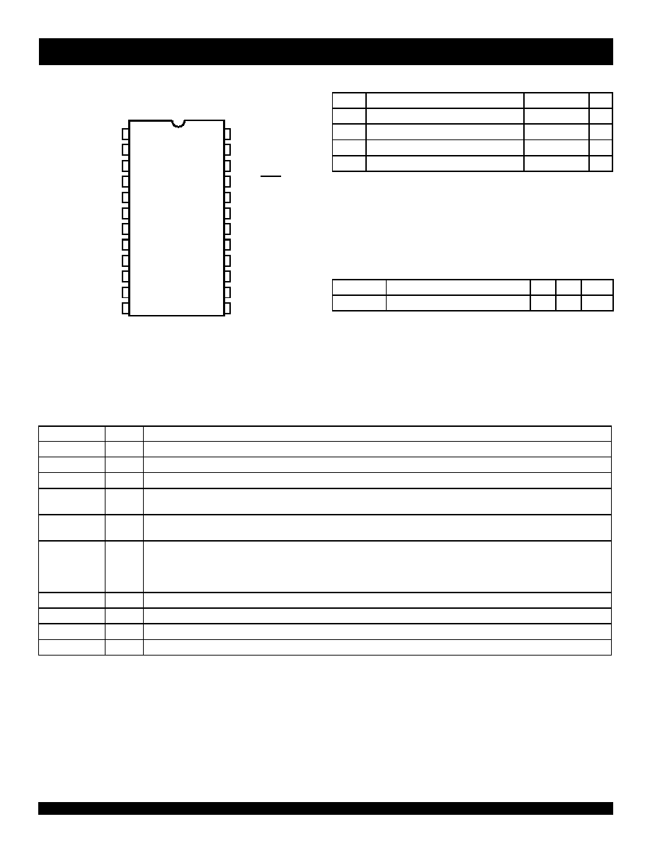
PIN CONFIGURATION
1
2
3
4
5
6
7
8
9
10
11
12
24
23
22
21
20
19
18
17
16
15
14
13
REF
FS
NC
VDDQ/P E
Q0
Q1
GND
Q2
Q3
GND
TE ST
NC
G ND/sO E
Q7
Q6
GND
Q5
Q4
FB
VDDN
V DDQ
V DDN
SO24-2
SOIC
TOP VIEW
ABSOLUTE MAXIMUM RATINGS (1)
Symbol
Rating
Max.
Unit
Supply Voltage to Ground
–0.5 to +7
V
VI
DC Input Voltage
–0.5 to +7
V
Maximum Power Dissipation (TA = 85°C)
530
mW
TSTG
Storage Temperature Range
–65°C to +150°C
°C
NOTE:
1. Stresses greater than those listed under ABSOLUTE MAXIMUM
RATINGS may cause permanent damage to the device. This is a
stress rating only and functional operation of the device at these or
any other conditions above those indicated in the operational sections
of this specification is not implied. Exposure to absolute maximum
rating conditions for extended periods may affect reliability.
CAPACITANCE (TA = 25° C, f = 1MHz, VIN = 0V)
Parameter
Description
Typ. Max.
Unit
CIN
Input Capacitance
5
7
pF
NOTE:
1. Capacitance applies to all inputs except TEST and FS. It is
characterized but not production tested.
PIN DESCRIPTION
Pin Name
Type
Description
REF
IN
Reference Clock Input
FB
IN
Feedback Input
TEST (1)
IN
When MID or HIGH, disables PLL (except for conditions of Note 1). REF goes to all outputs. Set LOW for normal operation.
GND/
sOE (1)
IN
Synchronous Output Enable. When HIGH, it stops clock outputs (Except Q2 and Q3) in a LOW state - Q2 and Q3 may be used as
the feedback signal to maintain phase lock. Set GND/
sOE LOW for normal operation.
VDDQ/PE
IN
Selectable positive or negative edge control. When LOW/HIGH the outputs are synchronized with the negative/positive edge of the
reference clock.
FS (2)
IN
Frequency range select. 3 level input.
FS = GND: 25 to 35MHz.
FS = MID (or open): 35 to 60MHz
FS = VDD: 60 to 85MHz
Q0 - Q7
OUT
8 clock output
VDDN
PWR
Power supply for output buffers
VDDQ
PWR
Power supply for phase locked loop and other internal circuitry
GND
PWR
Ground
NOTES:
1. When TEST = MID and GND/
sOE = HIGH, PLL remains active.
2. This input is wired to VDD, GND, or unconnected. Default is MID level. If it is switched in the real time mode, the outputs may glitch, and the PLL
may require an additional lock time before all data sheet limits are achieved.
相關(guān)PDF資料 |
PDF描述 |
|---|---|
| IDTCSPT855PGI8 | 855 SERIES, PLL BASED CLOCK DRIVER, 4 TRUE OUTPUT(S), 0 INVERTED OUTPUT(S), PDSO28 |
| IDTCSPT855PGG | 855 SERIES, PLL BASED CLOCK DRIVER, 4 TRUE OUTPUT(S), 0 INVERTED OUTPUT(S), PDSO28 |
| IDTCSPT855P | 855 SERIES, PLL BASED CLOCK DRIVER, 4 TRUE OUTPUT(S), 0 INVERTED OUTPUT(S), PDSO28 |
| IDTQS3125S1G | 3125 SERIES, 4-BIT DRIVER, TRUE OUTPUT, PDSO14 |
| IDTQS316245PV8 | DUAL 8-BIT DRIVER, TRUE OUTPUT, PDSO48 |
相關(guān)代理商/技術(shù)參數(shù) |
參數(shù)描述 |
|---|---|
| IDTCSPF2510C | 制造商:IDT 制造商全稱:Integrated Device Technology 功能描述:3.3V PHASE-LOCK LOOP CLOCK DRIVER |
| IDTCSPF2510CPG | 制造商:IDT 制造商全稱:Integrated Device Technology 功能描述:3.3V PHASE-LOCK LOOP CLOCK DRIVER |
| IDTCSPF2510CPGG | 制造商:IDT 制造商全稱:Integrated Device Technology 功能描述:3.3V PHASE-LOCK LOOP CLOCK DRIVER |
| IDTCSPF2510CPGGI | 制造商:IDT 制造商全稱:Integrated Device Technology 功能描述:3.3V PHASE-LOCK LOOP CLOCK DRIVER |
| IDTCSPF2510CPGI | 制造商:IDT 制造商全稱:Integrated Device Technology 功能描述:3.3V PHASE-LOCK LOOP CLOCK DRIVER |
發(fā)布緊急采購,3分鐘左右您將得到回復(fù)。