- 您現(xiàn)在的位置:買賣IC網(wǎng) > PDF目錄61104 > ILD32 (VISHAY SEMICONDUCTORS) 2 CHANNEL DARLINGTON OUTPUT OPTOCOUPLER PDF資料下載
參數(shù)資料
| 型號(hào): | ILD32 |
| 廠商: | VISHAY SEMICONDUCTORS |
| 元件分類: | 光電耦合器 |
| 英文描述: | 2 CHANNEL DARLINGTON OUTPUT OPTOCOUPLER |
| 封裝: | ROHS COMPLIANT, PLASTIC, DIP-8 |
| 文件頁數(shù): | 2/7頁 |
| 文件大?。?/td> | 160K |
| 代理商: | ILD32 |
www.vishay.com
For technical questions, contact: optocoupleranswers@vishay.com
Document Number: 83650
2
Rev. 1.7, 15-Feb-11
ILD32, ILQ32
Vishay Semiconductors
Optocoupler, Photodarlington Output,
High Gain (Dual, Quad Channel)
Note
Stresses in excess of the absolute maximum ratings can cause permanent damage to the device. Functional operation of the device is not
implied at these or any other conditions in excess of those given in the operational sections of this document. Exposure to absolute
maximum ratings for extended periods of the time can adversely affect reliability.
Note
Minimum and maximum values are testing requirements. Typical values are characteristics of the device and are the result of engineering
evaluation. Typical values are for information only and are not part of the testing requirements.
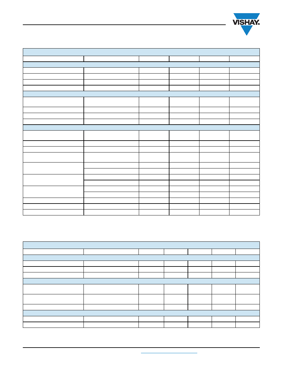
ABSOLUTE MAXIMUM RATINGS (Tamb = 25 °C, unless otherwise specified)
PARAMETER
TEST CONDITION
PART
SYMBOL
VALUE
UNIT
INPUT
Peak reverse voltage
VR
3V
Forward continuous current
IF
60
mA
Power dissipation
Pdiss
100
mW
Derate linearly from 25°C
1.33
mW/°C
OUTPUT
Collector emitter breakdown
voltage
BVCEO
30
V
Collector (load) current
IC
125
mA
Power dissipation
Pdiss
150
mW
Derate linearly from 25°C
2mW/°C
COUPLER
Isolation test voltage
between emitter and detector
t = 1 s
VISO
5300
VRMS
Creepage distance
7mm
Clearance distance
7mm
Comparative tracking index per
DIN IEC 112/VDE 0303, part 1
CTI
175
Isolation resistance
VIO = 500 V, Tamb = 25 °C
RIO
1012
VIO = 500 V, Tamb = 100 °C
RIO
1011
Total dissipation
ILD32
Ptot
400
mW
ILQ32
Ptot
500
mW
Derate linearly from 25 °C
ILD32
5.33
mW/°C
ILQ32
6.67
mW/°C
Storage temperature
Tstg
- 55 to + 150
°C
Operating temperature
Tamb
- 55 to + 100
°C
Lead soldering time at 260 °C
10
s
ELECTRICAL CHARACTERISTICS (Tamb = 25 °C, unless otherwise specified)
PARAMETER
TEST CONDITION
SYMBOL
MIN.
TYP.
MAX.
UNIT
INPUT
Forward voltage
IF = 10 mA
VF
1.25
1.5
V
Reverse current
VR = 3 V
IR
0.1
100
μA
Capacitance
VR = 0 V
CO
25
pF
OUTPUT
Collector emitter breakdown
voltage
IC = 100 A, IF = 0 A
BVCEO
30
V
Breakdown voltage emitter
collector
IE = 100 μA
BCECO
510
V
Collector emitter leakage current
VCE = 10 V, IF = 0 A
ICEO
1
100
nA
COUPLER
Collector emitter
IC = 2 mA, IF = 8 mA
VCEsat
1V
Capacitance (input to output)
CIO
0.5
pF
相關(guān)PDF資料 |
PDF描述 |
|---|---|
| ILQ32-X009T | 4 CHANNEL DARLINGTON OUTPUT OPTOCOUPLER |
| ILQ32-X009 | 4 CHANNEL DARLINGTON OUTPUT OPTOCOUPLER |
| ILD610-1-X016 | 2 CHANNEL TRANSISTOR OUTPUT OPTOCOUPLER |
| ILD610-2-X009 | 2 CHANNEL TRANSISTOR OUTPUT OPTOCOUPLER |
| ILD610-1-X016 | 2 CHANNEL TRANSISTOR OUTPUT OPTOCOUPLER |
相關(guān)代理商/技術(shù)參數(shù) |
參數(shù)描述 |
|---|---|
| ILD3-2 | 制造商:Vishay Angstrohm 功能描述:Optocoupler DC-IN 2-CH Darlington DC-OUT 8-Pin PDIP |
| ILD32-004 | 制造商:未知廠家 制造商全稱:未知廠家 功能描述:Optoelectronic |
| ILD32-009 | 制造商:未知廠家 制造商全稱:未知廠家 功能描述:Optoelectronic |
| ILD3-2X001 | 制造商:Vishay Angstrohm 功能描述:Optocoupler DC-IN 2-CH Transistor DC-OUT 8-Pin PDIP |
| ILD32-X006 | 制造商:VISHAY 制造商全稱:Vishay Siliconix 功能描述:Optocoupler, Photodarlington Output, High Gain (Dual, Quad Channel) |
發(fā)布緊急采購,3分鐘左右您將得到回復(fù)。