- 您現(xiàn)在的位置:買賣IC網(wǎng) > PDF目錄384535 > ISPGDX240VA-7B388I (LATTICE SEMICONDUCTOR CORP) In-System Programmable 3.3V Generic Digital CrosspointTM PDF資料下載
參數(shù)資料
| 型號: | ISPGDX240VA-7B388I |
| 廠商: | LATTICE SEMICONDUCTOR CORP |
| 元件分類: | PLD |
| 英文描述: | In-System Programmable 3.3V Generic Digital CrosspointTM |
| 中文描述: | EE PLD, 7 ns, PBGA388 |
| 封裝: | 23 X 23 MM, 1 MM PITCH, FPBGA-388 |
| 文件頁數(shù): | 5/25頁 |
| 文件大小: | 324K |
| 代理商: | ISPGDX240VA-7B388I |
5
Specifications
ispGDX240VA
ADVANCED
D30
D31
D28
D29
D30
D31
B24
B25
B26
B27
B28
B30
B31
B30
B31
B32
B33
D26
D27
D28
D29
D30
D31
D32
D33
B26
B27
B28
B29
B32
B33
B34
B35
D28
B31
B32
B33
B34
D27
D29
D30
D29
D30
D31
D32
B25
B26
B27
B29
B30
B31
B32
D25
D27
D28
D31
D32
D33
D34
B27
B28
B29
B28
B29
B30
B31
D24
D26
D27
D32
D33
D34
D35
B28
B29
B30
Data D/
MUXOUT
Data C/
MUXOUT
Data B/
MUXOUT
Data A/
MUXOUT
Reflected
I/O Cells
Normal
I/O Cells
Table 2. Adjacent I/O Cells (Mapping of
ispGDX240VA)
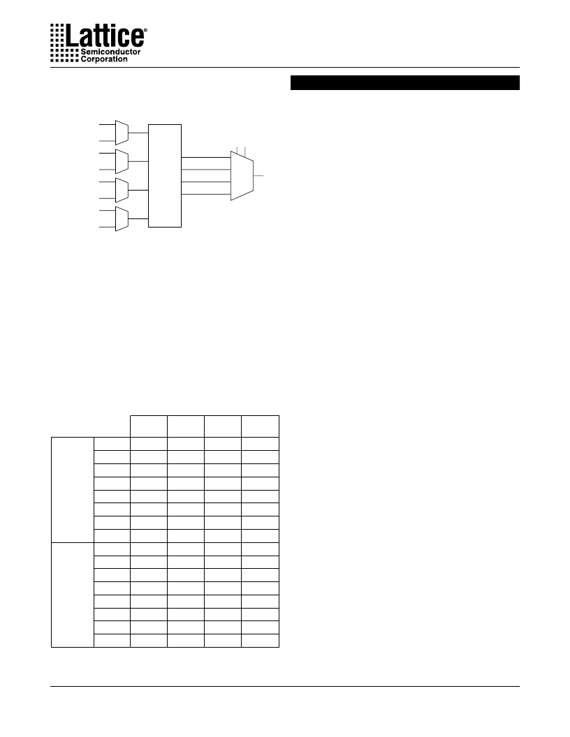
It can be seen from Figure 3 that if the D11 adjacent I/O
cell is used, the I/O group
“
”
input is no longer available
as a direct MUX input.
The ispGDXVA can implement MUXes up to 16 bits wide
in a single level of logic, but care must be taken when
combining adjacent I/O cell outputs with direct MUX
inputs. Any particular combination of adjacent I/O cells as
MUX inputs will dictate what I/O groups (A, B, C or D) can
be routed to the remaining inputs. By properly choosing
the adjacent I/O cells, all of the MUX inputs can be
utilized.
S0
S1
4 x 4
Crossbar
Switch
.m0
.m1
.m2
.m3
D33
I/O Group A
D31 MUX Out
I/O Group B
D32 MUX Out
I/O Group C
D34 MUX Out
I/O Group D
D35 MUX Out
ispGDX240VA I/O Cell
Figure 3. Adjacent I/O Cells vs. Direct Input Path for
ispGDX240VA, I/O D33
Special Features
Slew Rate Control
All output buffers contain a programmable slew rate
control that provides software-selectable slew rate op-
tions.
Open Drain Control
All output buffers provide a programmable Open-Drain
option which allows the user to drive system level reset,
need for an off-chip Open-Drain or Open-Collector buffer.
Wire-OR logic functions can be performed at the printed
circuit board level.
Pull-up Resistor
All pins have a programmable active pull-up. A typical
resistor value for the pull-up ranges from 50k
to 80k
.
Output Latch (Bus Hold)
All pins have a programmable circuit that weakly holds
the previously driven state when all drivers connected to
the pin (including the pin's output driver as well as any
other devices connected to the pin by external bus) are
tristated.
User-Programmable I/Os
The ispGDX240VA features user-programmable
I/Os supporting either 3.3V or 2.5V output voltage level
options. The ispGDX240VA uses a VCCIO pin to provide
the 2.5V reference voltage when used.
PCI Compatible Drive Capability
The ispGDX240VA supports PCI compatible drive capa-
bility for all I/Os.
相關PDF資料 |
PDF描述 |
|---|---|
| ISPGDX240VA-9B388I | In-System Programmable 3.3V Generic Digital CrosspointTM |
| ISPGDX80A-7T100 | In-System Programmable Generic Digital CrosspointTM |
| ISPGDX120A-5Q160 | In-System Programmable Generic Digital CrosspointTM |
| ISPGDX160A-5Q208 | In-System Programmable Generic Digital CrosspointTM |
| ISPGDX160-5Q208 | In-System Programmable Generic Digital CrosspointTM |
相關代理商/技術參數(shù) |
參數(shù)描述 |
|---|---|
| ISPGDX240VA-7BN388 | 功能描述:模擬和數(shù)字交叉點 IC PROGRAMMABLE GEN DIG CROSSPOINT RoHS:否 制造商:Micrel 配置:2 x 2 封裝 / 箱體:MLF-16 數(shù)據(jù)速率:10.7 Gbps 輸入電平:CML, LVDS, LVPECL 輸出電平:CML 電源電壓-最大:3.6 V 電源電壓-最小:2.375 V 最大工作溫度:+ 85 C 最小工作溫度:- 40 C 產(chǎn)品:Digital Crosspoint 封裝:Tube |
| ISPGDX240VA-7BN388I | 功能描述:模擬和數(shù)字交叉點 IC PROGRAMMABLE GEN DIG CROSSPOINT RoHS:否 制造商:Micrel 配置:2 x 2 封裝 / 箱體:MLF-16 數(shù)據(jù)速率:10.7 Gbps 輸入電平:CML, LVDS, LVPECL 輸出電平:CML 電源電壓-最大:3.6 V 電源電壓-最小:2.375 V 最大工作溫度:+ 85 C 最小工作溫度:- 40 C 產(chǎn)品:Digital Crosspoint 封裝:Tube |
| ISPGDX240VA-9B388I | 制造商:LATTICE 制造商全稱:Lattice Semiconductor 功能描述:In-System Programmable 3.3V Generic Digital CrosspointTM |
| ISPGDX2-64/E | 制造商:LATTICE 制造商全稱:Lattice Semiconductor 功能描述:High Performance Interfacing and Switching |
| ISPGDX80A-5T100 | 功能描述:模擬和數(shù)字交叉點 IC PROGRAMMABLE GEN DIG CROSSPOINT RoHS:否 制造商:Micrel 配置:2 x 2 封裝 / 箱體:MLF-16 數(shù)據(jù)速率:10.7 Gbps 輸入電平:CML, LVDS, LVPECL 輸出電平:CML 電源電壓-最大:3.6 V 電源電壓-最小:2.375 V 最大工作溫度:+ 85 C 最小工作溫度:- 40 C 產(chǎn)品:Digital Crosspoint 封裝:Tube |
發(fā)布緊急采購,3分鐘左右您將得到回復。