- 您現(xiàn)在的位置:買(mǎi)賣(mài)IC網(wǎng) > PDF目錄374254 > K4B1G0446C (SAMSUNG SEMICONDUCTOR CO. LTD.) 1Gb C-die DDR3 SDRAM Specification PDF資料下載
參數(shù)資料
| 型號(hào): | K4B1G0446C |
| 廠商: | SAMSUNG SEMICONDUCTOR CO. LTD. |
| 英文描述: | 1Gb C-die DDR3 SDRAM Specification |
| 中文描述: | 1Gb的?芯片的DDR3 SDRAM規(guī)范 |
| 文件頁(yè)數(shù): | 33/63頁(yè) |
| 文件大小: | 1255K |
| 代理商: | K4B1G0446C |
第1頁(yè)第2頁(yè)第3頁(yè)第4頁(yè)第5頁(yè)第6頁(yè)第7頁(yè)第8頁(yè)第9頁(yè)第10頁(yè)第11頁(yè)第12頁(yè)第13頁(yè)第14頁(yè)第15頁(yè)第16頁(yè)第17頁(yè)第18頁(yè)第19頁(yè)第20頁(yè)第21頁(yè)第22頁(yè)第23頁(yè)第24頁(yè)第25頁(yè)第26頁(yè)第27頁(yè)第28頁(yè)第29頁(yè)第30頁(yè)第31頁(yè)第32頁(yè)當(dāng)前第33頁(yè)第34頁(yè)第35頁(yè)第36頁(yè)第37頁(yè)第38頁(yè)第39頁(yè)第40頁(yè)第41頁(yè)第42頁(yè)第43頁(yè)第44頁(yè)第45頁(yè)第46頁(yè)第47頁(yè)第48頁(yè)第49頁(yè)第50頁(yè)第51頁(yè)第52頁(yè)第53頁(yè)第54頁(yè)第55頁(yè)第56頁(yè)第57頁(yè)第58頁(yè)第59頁(yè)第60頁(yè)第61頁(yè)第62頁(yè)第63頁(yè)
Page 33 of 63
Rev. 1.0 June 2007
1Gb DDR3 SDRAM
K4B1G04(08/16)46C
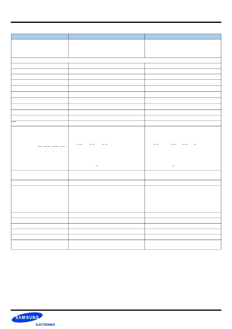
[ Table 34 ] IDD Measurement Conditions for IDD0 and IDD1
Current
IDD0
IDD1
Name
Operating Current 0
-> One Bank Activate
-> Precharge
Operating Current 1
-> One Bank Activate
-> Read
-> Precharge
Measurement Condition
Timing Diagram Example
Figure 1
CKE
HIGH
HIGH
External Clock
on
on
t
CK
t
CK
min(IDD)
t
CK
min(IDD)
t
RC
t
RC
min(IDD)
t
RC
min(IDD)
t
RAS
t
RAS
min(IDD)
t
RAS
min(IDD)
t
RCD
n.a.
t
RCD
min(IDD)
t
RRD
n.a.
n.a.
CL
n.a.
CL(IDD)
AL
n.a.
0
CS
HIGH between. Activate and Precharge Commands
HIGH between Activate, Read and Precharge
Command Inputs (CS, RAS, CAS, WE)
SWITCHING as described in Table 2;
only exceptions are Activate and Precharge com-
mands; example of IDD0 pattern:
A0 D D D D D D D D D D D
P0
(DDR3-800: tRAS = 37.5ns between (A)ctivate and
(P)recharge to bank 0 ; Definition of D and D: see
Table 2)
Definition of D and D: See table ##.
SWITCHING as described in Table 2;
only exceptions are Activate, Read and Precharge
commands; example of IDD1 pattern:
A0 D D D D R0 D D D DD D D DD D
P0
(DDR3-800 -555: tRCD = 12.5ns between (A)ctivate
and (R)ead to bank 0 ; Definition of D and D: see Table
2)
Definition of D and D: See table ##.
Row, Column Addresses
Row addresses SWITCHING as described in Table 2;
Address Input A10 must be LOW all the time!
Row addresses SWITCHING as described in Table 2;
Address Input A10 must be LOW all the time!
Bank Addresses
bank address is fixed (bank 0)
bank address is fixed (bank 0)
Data I/O
SWITCHING as described in Table 3
Read Data: output data switches every clock, which
means that Read data is stable during one clock cycle.
To achieve Iout = 0mA the output buffer should be
switched off by MR1 Bit A12 set to "1".
When there is no read data burst from DRAM the DQ
I/O should be FLOATING.
Output Buffer DQ,DQS / MR1 bit A12
off / 1
off / 1
Rtt_NOM, Rtt_WR
disabled
disabled
Burst length
n.a.
8 fixed / MR0 Bits [A1, A0] = {0,0}
Active banks
one ACT-PRE loop
one ACT-RD-PRE loop
Idle banks
all other
all other
Precharge Power Down Mode /
Mode Register Bit 12
n.a.
n.a.
相關(guān)PDF資料 |
PDF描述 |
|---|---|
| K4B1G0446C-CF8 | 1Gb C-die DDR3 SDRAM Specification |
| K4B1G0446C-ZCF7 | 1Gb C-die DDR3 SDRAM Specification |
| K4B1G0446C-ZCG9 | 1Gb C-die DDR3 SDRAM Specification |
| K4B1G0846C-CF8 | 1Gb C-die DDR3 SDRAM Specification |
| K4B1G0846C-ZCF7 | 1Gb C-die DDR3 SDRAM Specification |
相關(guān)代理商/技術(shù)參數(shù) |
參數(shù)描述 |
|---|---|
| K4B1G0446C-CF8 | 制造商:SAMSUNG 制造商全稱:Samsung semiconductor 功能描述:1Gb C-die DDR3 SDRAM Specification |
| K4B1G0446C-ZCF7 | 制造商:SAMSUNG 制造商全稱:Samsung semiconductor 功能描述:1Gb C-die DDR3 SDRAM Specification |
| K4B1G0446C-ZCG9 | 制造商:SAMSUNG 制造商全稱:Samsung semiconductor 功能描述:1Gb C-die DDR3 SDRAM Specification |
| K4B1G0446D | 制造商:SAMSUNG 制造商全稱:Samsung semiconductor 功能描述:1Gb D-die DDR3 SDRAM Specification |
| K4B1G0446D-HCF7 | 制造商:SAMSUNG 制造商全稱:Samsung semiconductor 功能描述:1Gb D-die DDR3 SDRAM Specification |
發(fā)布緊急采購(gòu),3分鐘左右您將得到回復(fù)。