- 您現(xiàn)在的位置:買賣IC網(wǎng) > PDF目錄374254 > K4B1G0846C-CF8 (SAMSUNG SEMICONDUCTOR CO. LTD.) 1Gb C-die DDR3 SDRAM Specification PDF資料下載
參數(shù)資料
| 型號(hào): | K4B1G0846C-CF8 |
| 廠商: | SAMSUNG SEMICONDUCTOR CO. LTD. |
| 英文描述: | 1Gb C-die DDR3 SDRAM Specification |
| 中文描述: | 1Gb的?芯片的DDR3 SDRAM規(guī)范 |
| 文件頁數(shù): | 48/63頁 |
| 文件大小: | 1255K |
| 代理商: | K4B1G0846C-CF8 |
第1頁第2頁第3頁第4頁第5頁第6頁第7頁第8頁第9頁第10頁第11頁第12頁第13頁第14頁第15頁第16頁第17頁第18頁第19頁第20頁第21頁第22頁第23頁第24頁第25頁第26頁第27頁第28頁第29頁第30頁第31頁第32頁第33頁第34頁第35頁第36頁第37頁第38頁第39頁第40頁第41頁第42頁第43頁第44頁第45頁第46頁第47頁當(dāng)前第48頁第49頁第50頁第51頁第52頁第53頁第54頁第55頁第56頁第57頁第58頁第59頁第60頁第61頁第62頁第63頁
Page 48 of 63
Rev. 1.0 June 2007
1Gb DDR3 SDRAM
K4B1G04(08/16)46C
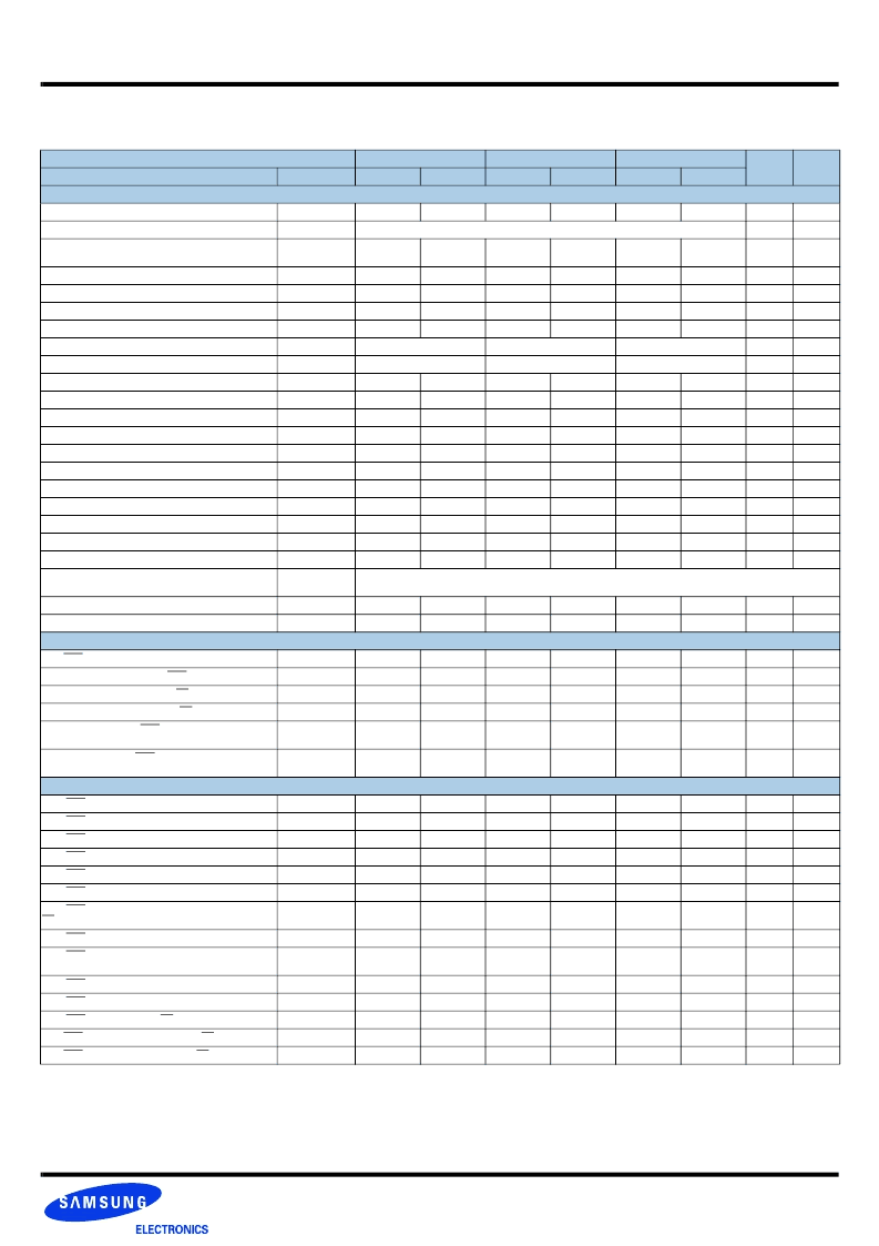
[ Table 51 ] Timing Parameters by Speed Bin
Speed
DDR3-800
DDR3-1066
DDR3-1333
Units
Note
Parameter
Symbol
MIN
MAX
MIN
MAX
MIN
MAX
Clock Timing
Minimum Clock Cycle Time (DLL off mode)
t
CK(DLL_OFF)
8
-
8
-
8
-
ns
6
Average Clock Period
t
CK(avg)
See Speed Bins Table
ps
f
Clock Period
t
CK(abs)
tCK(avg)min +
tJIT(per)min
tCK(avg)max +
tJIT(per)max
tCK(avg)min +
tJIT(per)min
tCK(avg)max +
tJIT(per)max
tCK(avg)min +
tJIT(per)min
tCK(avg)max +
tJIT(per)max
ps
Average high pulse width
t
CH(avg)
0.47
0.53
0.47
0.53
0.47
0.53
t
CK(avg)
f
Average low pulse width
t
CL(avg)
0.47
0.53
0.47
0.53
0.47
0.53
t
CK(avg)
f
Clock Period Jitter
tJIT
(per)
-100
100
-90
90
-80
80
ps
Clock Period Jitter during DLL locking period
tJIT
(per, lck)
-90
90
-80
80
-70
70
ps
Cycle to Cycle Period Jitter
tJIT
(cc)
200
180
160
ps
Cycle to Cycle Period Jitter during DLL locking period
tJIT
(cc, lck)
180
160
140
ps
Cumulative error across 2 cycles
t
ERR(2per)
- 147
147
- 132
132
- 118
118
ps
Cumulative error across 3 cycles
t
ERR(3per)
- 175
175
- 157
157
- 140
140
ps
Cumulative error across 4 cycles
t
ERR(4per)
- 194
194
- 175
175
- 155
155
ps
Cumulative error across 5 cycles
t
ERR(5per)
- 209
209
- 188
188
- 168
168
ps
Cumulative error across 6 cycles
t
ERR(6per)
- 222
222
- 200
200
- 177
177
ps
Cumulative error across 7 cycles
t
ERR(7per)
- 232
232
- 209
209
- 186
186
ps
Cumulative error across 8 cycles
t
ERR(8per)
- 241
241
- 217
217
- 193
193
ps
Cumulative error across 9 cycles
t
ERR(9per)
- 249
249
- 224
224
- 200
200
ps
Cumulative error across 10 cycles
t
ERR(10per)
- 257
257
- 231
231
- 205
205
ps
Cumulative error across 11 cycles
t
ERR(11per)
- 263
263
- 237
237
- 210
210
ps
Cumulative error across 12 cycles
t
ERR(12per)
- 269
269
- 242
242
- 215
215
PS
Cumulative error across n = 13, 14 ... 49, 50 cycles
t
ERR(nper)
tERR(nper)min = (1 + 0.68ln(n))*tJIT(per)min
tERR(nper)max = (1 = 0.68ln(n))*tJIT(per)max
Absolute clock HIGH pulse width
t
CH(abs)
0.43
0.43
0.43
t
CK(avg)
25
Absolute clock Low pulse width
t
CL(abs)
0.43
0.43
0.43
t
CK(avg)
26
Data Timing
DQS,DQS to DQ skew, per group, per access
t
DQSQ
-
200
-
150
-
125
ps
12,13
DQ output hold time from DQS, DQS
t
QH
0.38
-
0.38
-
0.38
-
t
CK(avg)
12,13
DQ low-impedance time from CK, CK
t
LZ(DQ)
-800
400
-600
300
-500
250
ps
13,14, a
DQ high-impedance time from CK, CK
t
HZ(DQ)
-
400
-
300
-
250
ps
13,14, a
Data setup time to DQS, DQS referenced to Vih(ac)Vil(ac)
levels
t
DS(base)
75
-
25
-
-10
-
ps
d, 17
Data hold time to DQS, DQS referenced to Vih(ac)Vil(ac)
levels
t
DH(base)
150
-
100
-
65
-
ps
d, 17
Data Strobe Timing
DQS, DQS READ Preamble
t
RPRE
0.9
-
0.9
-
0.9
-
t
CK
13, 19, b
DQS, DQS differential READ Postamble
t
RPST
0.3
NOTE1
0.3
NOTE1
0.3
NOTE1
t
CK
11, 13, b
DQS, DQS output high time
t
QSH
0.38
-
0.38
-
0.4
-
t
CK(avg)
13, b
DQS, DQS output low time
t
QSL
0.38
-
0.38
-
0.4
-
t
CK(avg)
13, b
DQS, DQS WRITE Preamble
t
WPRE
0.9
-
0.9
-
0.9
-
t
CK
1
DQS, DQS WRITE Postamble
t
WPST
0.3
-
0.3
-
0.3
-
t
CK
1
DQS, DQS rising edge output access time from rising CK,
CK
t
DQSCK
-400
400
-300
300
-255
255
ps
12,13
DQS, DQS low-impedance time (Referenced from RL-1)
t
LZ(DQS)
-800
400
-600
300
-500
250
ps
12,13,14
DQS, DQS high-impedance time (Referenced from RL+BL/
2)
t
HZ(DQS)
-
400
-
300
-
250
ps
12,13,14
DQS, DQS differential input low pulse width
t
DQSL
0.4
0.6
0.4
0.6
0.4
0.6
t
CK
DQS, DQS differential input high pulse width
t
DQSH
0.4
0.6
0.4
0.6
0.4
0.6
t
CK
DQS, DQS rising edge to CK, CK rising edge
t
DQSS
-0.25
0.25
-0.25
0.25
-0.25
0.25
t
CK(avg)
c
DQS,DQS faling edge setup time to CK, CK rising edge
t
DSS
0.2
-
0.2
-
0.2
-
t
CK(avg)
c
DQS,DQS faling edge hold time to CK, CK rising edge
t
DSH
0.2
-
0.2
-
0.2
-
t
CK(avg)
c
13.0 Timing Parameters by Speed Grade
相關(guān)PDF資料 |
PDF描述 |
|---|---|
| K4B1G0846C-ZCF7 | 1Gb C-die DDR3 SDRAM Specification |
| K4B1G0846C-ZCG9 | 1Gb C-die DDR3 SDRAM Specification |
| K4B1G1646C-CF8 | 1Gb C-die DDR3 SDRAM Specification |
| K4B1G1646C-ZCF7 | 1Gb C-die DDR3 SDRAM Specification |
| K4B1G1646C-ZCG9 | 1Gb C-die DDR3 SDRAM Specification |
相關(guān)代理商/技術(shù)參數(shù) |
參數(shù)描述 |
|---|---|
| K4B1G0846C-ZCF7 | 制造商:SAMSUNG 制造商全稱:Samsung semiconductor 功能描述:1Gb C-die DDR3 SDRAM Specification |
| K4B1G0846C-ZCG9 | 制造商:SAMSUNG 制造商全稱:Samsung semiconductor 功能描述:1Gb C-die DDR3 SDRAM Specification |
| K4B1G0846D | 制造商:SAMSUNG 制造商全稱:Samsung semiconductor 功能描述:1Gb D-die DDR3 SDRAM Specification |
| K4B1G0846D-HCF7 | 制造商:SAMSUNG 制造商全稱:Samsung semiconductor 功能描述:1Gb D-die DDR3 SDRAM Specification |
| K4B1G0846D-HCF8 | 制造商:SAMSUNG 制造商全稱:Samsung semiconductor 功能描述:1Gb D-die DDR3 SDRAM Specification |
發(fā)布緊急采購,3分鐘左右您將得到回復(fù)。