- 您現(xiàn)在的位置:買賣IC網(wǎng) > PDF目錄374254 > K4B1G0846C-ZCF7 (SAMSUNG SEMICONDUCTOR CO. LTD.) 1Gb C-die DDR3 SDRAM Specification PDF資料下載
參數(shù)資料
| 型號: | K4B1G0846C-ZCF7 |
| 廠商: | SAMSUNG SEMICONDUCTOR CO. LTD. |
| 英文描述: | 1Gb C-die DDR3 SDRAM Specification |
| 中文描述: | 1Gb的?芯片的DDR3 SDRAM規(guī)范 |
| 文件頁數(shù): | 47/63頁 |
| 文件大小: | 1255K |
| 代理商: | K4B1G0846C-ZCF7 |
第1頁第2頁第3頁第4頁第5頁第6頁第7頁第8頁第9頁第10頁第11頁第12頁第13頁第14頁第15頁第16頁第17頁第18頁第19頁第20頁第21頁第22頁第23頁第24頁第25頁第26頁第27頁第28頁第29頁第30頁第31頁第32頁第33頁第34頁第35頁第36頁第37頁第38頁第39頁第40頁第41頁第42頁第43頁第44頁第45頁第46頁當(dāng)前第47頁第48頁第49頁第50頁第51頁第52頁第53頁第54頁第55頁第56頁第57頁第58頁第59頁第60頁第61頁第62頁第63頁
Page 47 of 63
Rev. 1.0 June 2007
1Gb DDR3 SDRAM
K4B1G04(08/16)46C
NOTES
:
Absolute Specification (TOPER;VDDQ=VDD=1.5V +/- 0.075V);
1. The CL setting and CWL setting result in tCK(AVG).MIN and tCK(AVG).MAX requirements. When making a selection of tCK(AVG), both need to be ful-
filed: Requirements from CL setting as well as requirements from CWL setting.
2. tCK(AVG).MIN limits: Since CAS Latency is not purely analog - data and strobe output are synchronized by the DLL - all possible intermediate frequen-
cies may not be guaranteed. An application should use the next smaller JEDEC standard tCK(AVG) value (2.5, 1.875, 1.5, or 1.25 ns) when calculat-
ing CL [nCK] = tAA [ns] / tCK(AVG) [ns], rounding up to the next ’Supported CL’.
3. tCK(AVG).MAX limits: Calculate tCK(AVG) = tAA.MAX / CLSELECTED and round the resulting tCK(AVG) down to the next valid speed bin limit (i.e.
3.3ns or 2.5ns or 1.875 ns or 1.25 ns). This result is tCK(AVG).MAX corresponding to CLSELECTED.
4. ’Reserved’ settings are not allowed. User must program a different value.
5. ’Optional’ settings allow certain devices in the industry to support this setting, however, it is not a mandatory feature. Refer to supplier’s data sheet and
SPD information if and how this setting is supported.
6. Any DDR3-1066 speed bin also supports functional operation at lower frequencies as shown in the table which are not subject to Production Tests but
verified by Design/Characterization.
7. Any DDR3-1333 speed bin also supports functional operation at lower frequencies as shown in the table which are not subject to Production Tests but
verified by Design/Characterization.
8. tREFI depends on TOPER
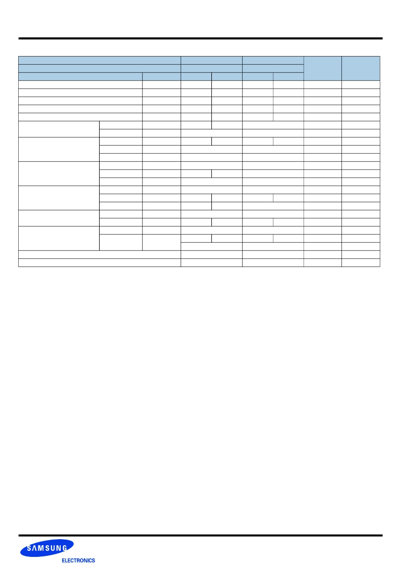
[ Table 50 ] DDR3-1333 Speed Bins
Speed
DDR3-1333
8 - 8 - 8
min
12
12
12
48
36
2.5
Reserved
2.5
Reserved
Reserved
Reserved
1.875
Reserved
Reserved
1.875
1.5
Reserved
1.5
Reserved
1.5
(Optional)
5,6,7,8,9
5,6,7
DDR3-1333
9 -9 - 9
min
13.5
13.5
13.5
49.5
36
Reserved
Reserved
2.5
Reserved
Reserved
Reserved
Reserved
Reserved
Reserved
1.875
Reserved
Reserved
1.5
Reserved
1.5
(Optional)
6,8,9
5,6,7
Units
Note
CL-nRCD-nRP
Parameter
Symbol
t
AA
t
RCD
t
RP
t
RC
t
RAS
t
CK(AVG)
t
CK(AVG)
t
CK(AVG)
t
CK(AVG)
t
CK(AVG)
t
CK(AVG)
t
CK(AVG)
t
CK(AVG)
t
CK(AVG)
t
CK(AVG)
t
CK(AVG)
t
CK(AVG)
t
CK(AVG)
t
CK(AVG)
max
20
-
-
-
9*tREFI
3.3
max
20
-
-
-
9*tREFI
Intermal read command to first data
ACT to internal read or write delay time
PRE command period
ACT to ACT or REF command period
ACT to PRE command period
ns
ns
ns
ns
ns
ns
ns
ns
ns
ns
ns
ns
ns
ns
ns
ns
ns
ns
ns
ns
ns
n
CK
n
CK
8
CL = 5
CWL = 5
CWL = 6,7
CWL = 5
CWL = 6
CWL = 7
CWL = 5
CWL = 6
CWL = 7
CWL = 5
CWL = 6
CWL = 7
CWL = 5,6
CWL = 7
CWL = 5,6
1,2,3,4,7
4
1,2,3,7
1,2,3,4,7
4
4
1,2,3,4,7
1,2,3,4,
4
1,2,3,7
1,2,3,4,
4
1,2,3,4
4
1,2,3
5
CL = 6
3.3
3.3
CL = 7
<2.5
CL = 8
<2.5
<1.875
<2.5
CL = 9
<1.875
<1.875
CL = 10
CWL = 7
t
CK(AVG)
<1.875
<1.875
Supported CL Settings
Supported CWL Settings
相關(guān)PDF資料 |
PDF描述 |
|---|---|
| K4B1G0846C-ZCG9 | 1Gb C-die DDR3 SDRAM Specification |
| K4B1G1646C-CF8 | 1Gb C-die DDR3 SDRAM Specification |
| K4B1G1646C-ZCF7 | 1Gb C-die DDR3 SDRAM Specification |
| K4B1G1646C-ZCG9 | 1Gb C-die DDR3 SDRAM Specification |
| K4C560838C-TCD3 | 256Mb Network-DRAM |
相關(guān)代理商/技術(shù)參數(shù) |
參數(shù)描述 |
|---|---|
| K4B1G0846C-ZCG9 | 制造商:SAMSUNG 制造商全稱:Samsung semiconductor 功能描述:1Gb C-die DDR3 SDRAM Specification |
| K4B1G0846D | 制造商:SAMSUNG 制造商全稱:Samsung semiconductor 功能描述:1Gb D-die DDR3 SDRAM Specification |
| K4B1G0846D-HCF7 | 制造商:SAMSUNG 制造商全稱:Samsung semiconductor 功能描述:1Gb D-die DDR3 SDRAM Specification |
| K4B1G0846D-HCF8 | 制造商:SAMSUNG 制造商全稱:Samsung semiconductor 功能描述:1Gb D-die DDR3 SDRAM Specification |
| K4B1G0846D-HCH9 | 制造商:SAMSUNG 制造商全稱:Samsung semiconductor 功能描述:1Gb D-die DDR3 SDRAM Specification |
發(fā)布緊急采購,3分鐘左右您將得到回復(fù)。