- 您現(xiàn)在的位置:買賣IC網(wǎng) > PDF目錄374254 > K4B1G0846C-ZCG9 (SAMSUNG SEMICONDUCTOR CO. LTD.) 1Gb C-die DDR3 SDRAM Specification PDF資料下載
參數(shù)資料
| 型號: | K4B1G0846C-ZCG9 |
| 廠商: | SAMSUNG SEMICONDUCTOR CO. LTD. |
| 英文描述: | 1Gb C-die DDR3 SDRAM Specification |
| 中文描述: | 1Gb的?芯片的DDR3 SDRAM規(guī)范 |
| 文件頁數(shù): | 4/63頁 |
| 文件大小: | 1255K |
| 代理商: | K4B1G0846C-ZCG9 |
第1頁第2頁第3頁當前第4頁第5頁第6頁第7頁第8頁第9頁第10頁第11頁第12頁第13頁第14頁第15頁第16頁第17頁第18頁第19頁第20頁第21頁第22頁第23頁第24頁第25頁第26頁第27頁第28頁第29頁第30頁第31頁第32頁第33頁第34頁第35頁第36頁第37頁第38頁第39頁第40頁第41頁第42頁第43頁第44頁第45頁第46頁第47頁第48頁第49頁第50頁第51頁第52頁第53頁第54頁第55頁第56頁第57頁第58頁第59頁第60頁第61頁第62頁第63頁
Page 4 of 63
Rev. 1.0 June 2007
1Gb DDR3 SDRAM
K4B1G04(08/16)46C
JEDEC standard 1.5V ± 0.075V Power Supply
VDDQ = 1.5V ± 0.075V
400 MHz f
CK
for 800Mb/sec/pin, 533MHz f
CK
for 1066Mb/sec/pin,
667MHz f
CK
for 1333Mb/sec/pin
8 Banks
Posted CAS
Programmable CAS Latency: 5, 6, 7, 8, 9, 10, (11 for high density
only)
Programmable Additive Latency: 0, CL-2 or CL-1 clock
Programmable CAS Write Latency (CWL) = 5 (DDR3-800), 6
(DDR3-1066), 7 (DDR3-1333)
8-bit pre-fetch
Burst Length: 8 (Interleave without any limit, sequential with starting
address “000” only), 4 with tCCD = 4 which does not allow seamless
read or write [either On the fly using A12 or MRS]
Bi-directional Differential Data-Strobe
Internal(self) calibration : Internal self calibration through ZQ pin
(RZQ : 240 ohm ± 1%)
On Die Termination using ODT pin
Average Refresh Period 7.8us at lower than T
CASE
85×C, 3.9us at
85×C < T
CASE
< 95 ×C
Asynchronous Reset
Package : 94 balls FBGA - x4/x8 (with 16 support balls)
112 balls FBGA - x16 (with 16 support balls)
All of Lead-free products are compliant for RoHS
The 1Gb DDR3 SDRAM C-die is organized as a 32Mbit x 4/16Mbit x 8/
8Mbit x 16 I/Os x 8banks device. This synchronous device achieves high
speed double-data-rate transfer rates of up to 1333Mb/sec/pin (DDR3-
1333) for general applications.
The chip is designed to comply with the following key DDR3 SDRAM fea-
tures such as posted CAS, Programmable CWL, Internal (Self) Calibra-
tion, On Die Termination using ODT pin and Asynchronous Reset .
All of the control and address inputs are synchronized with a pair of exter-
nally supplied differential clocks. Inputs are latched at the crosspoint of dif-
ferential clocks (CK rising and CK falling). All I/Os are synchronized with a
pair of bidirectional strobes (DQS and DQS) in a source synchronous fash-
ion. The address bus is used to convey row, column, and bank address
information in a RAS/CAS multiplexing style. The DDR3 device operates
with a single 1.5V ± 0.075V power supply and 1.5V ± 0.075V VDDQ.
The 1Gb DDR3 device is available in 94ball FBGAs(x4/x8) and 112ball
FBGA(x16)
Note : 1. The functionality described and the timing specifications included
in this data sheet are for the DLL Enabled mode of operation.
2. 1066Mbps CL7 doesn’t have back-ward compatibility with
800Mbps CL5
Note : This data sheet is an abstract of full DDR3 specification and does not cover the common features which are described in “DDR3 SDRAM Device
Operation & Timing Diagram”.
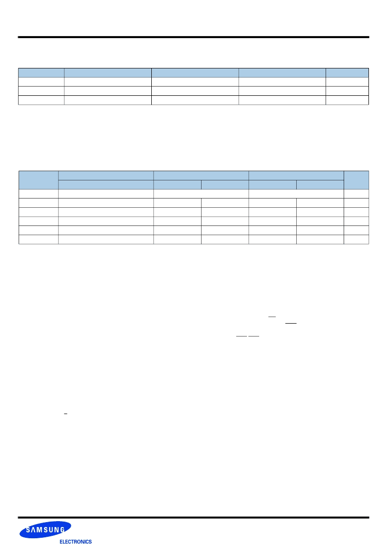
[ Table 1 ] Samsung DDR3 ordering information table
Note :
1. Speed bin is in order of CL-tRCD-tRP.
2. x4/x8/x16 Package - including 16 support balls
Organization
DDR3-800 (6-6-6)
DDR3-1066 (7-7-7/8-8-8)
DDR3-1333 (8-8-8/9-9-9)
Package
256Mx4
K4B1G0446C-ZCF7
K4B1G0446C-CF8/G8
K4B1G0446C-ZCG9/H9
94 FBGA
128Mx8
K4B1G0846C-ZCF7
K4B1G0846C-CF8/G8
K4B1G0846C-ZCG9/H9
94 FBGA
64Mx16
K4B1G1646C-ZCF7
K4B1G1646C-CF8/G8
K4B1G1646C-ZCG9/H9
112 FBGA
[ Table 2 ] 1Gb DDR3 C-die Speed bins
Speed
DDR3-800
DDR3-1066
DDR3-1333
Unit
6-6-6
7-7-7
8-8-8
8-8-8
9-9-9
tCK(min)
2.5
1.875
1.5
ns
CAS Latency
6
7
8
8
9
tCK
tRCD(min)
15
13.125
15
12
13.5
ns
tRP(min)
15
13.125
15
12
13.5
ns
tRAS(min)
37.5
37.5
37.5
36
36
ns
tRC(min)
52.5
50.625
52.5
48
49.5
ns
1.0 Ordering Information
2.0 Key Features
相關(guān)PDF資料 |
PDF描述 |
|---|---|
| K4B1G1646C-CF8 | 1Gb C-die DDR3 SDRAM Specification |
| K4B1G1646C-ZCF7 | 1Gb C-die DDR3 SDRAM Specification |
| K4B1G1646C-ZCG9 | 1Gb C-die DDR3 SDRAM Specification |
| K4C560838C-TCD3 | 256Mb Network-DRAM |
| K4C560838C-TCD4 | Aluminum Electrolytic Radial Lead High Ripple, Long Life Capacitor; Capacitance: 150uF; Voltage: 200V; Case Size: 16x31.5 mm; Packaging: Bulk |
相關(guān)代理商/技術(shù)參數(shù) |
參數(shù)描述 |
|---|---|
| K4B1G0846D | 制造商:SAMSUNG 制造商全稱:Samsung semiconductor 功能描述:1Gb D-die DDR3 SDRAM Specification |
| K4B1G0846D-HCF7 | 制造商:SAMSUNG 制造商全稱:Samsung semiconductor 功能描述:1Gb D-die DDR3 SDRAM Specification |
| K4B1G0846D-HCF8 | 制造商:SAMSUNG 制造商全稱:Samsung semiconductor 功能描述:1Gb D-die DDR3 SDRAM Specification |
| K4B1G0846D-HCH9 | 制造商:SAMSUNG 制造商全稱:Samsung semiconductor 功能描述:1Gb D-die DDR3 SDRAM Specification |
| K4B1G0846E | 制造商:SAMSUNG 制造商全稱:Samsung semiconductor 功能描述:Consumer Memory |
發(fā)布緊急采購,3分鐘左右您將得到回復。