- 您現(xiàn)在的位置:買賣IC網(wǎng) > PDF目錄374276 > K4M511633E-F1L (SAMSUNG SEMICONDUCTOR CO. LTD.) 8M x 16Bit x 4 Banks Mobile SDRAM in 54FBGA PDF資料下載
參數(shù)資料
| 型號: | K4M511633E-F1L |
| 廠商: | SAMSUNG SEMICONDUCTOR CO. LTD. |
| 英文描述: | 8M x 16Bit x 4 Banks Mobile SDRAM in 54FBGA |
| 中文描述: | 8米× 16 × 4銀行在54FBGA移動SDRAM |
| 文件頁數(shù): | 3/12頁 |
| 文件大?。?/td> | 112K |
| 代理商: | K4M511633E-F1L |
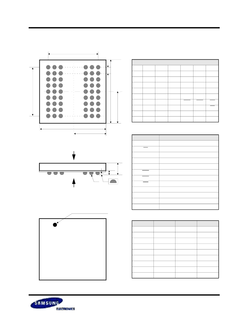
K4M511633E - Y(P)C/L/F
February 2004
Mobile-SDRAM
54Ball(6x9) FBGA
1
2
3
7
8
9
A
VSS
DQ15
VSSQ
VDDQ
DQ0
VDD
B
DQ14
DQ13
VDDQ
VSSQ
DQ2
DQ1
C
DQ12
DQ11
VSSQ
VDDQ
DQ4
DQ3
D
DQ10
DQ9
VDDQ
VSSQ
DQ6
DQ5
E
DQ8
NC
VSS
VDD
LDQM
DQ7
F
UDQM
CLK
CKE
CAS
RAS
WE
G
A12
A11
A9
BA0
BA1
CS
H
A8
A7
A6
A0
A1
A10
J
VSS
A5
A4
A3
A2
VDD
Pin Name
Pin Function
CLK
System Clock
CS
Chip Select
CKE
Clock Enable
A
0
~ A
12
Address
BA
0
~ BA
1
Bank Select Address
RAS
Row Address Strobe
CAS
Column Address Strobe
WE
Write Enable
L(U)DQM
Data Input/Output Mask
DQ
0
~
15
Data Input/Output
V
DD
/V
SS
Power Supply/Ground
V
DDQ
/V
SSQ
Data Output Power/Ground
Symbol
Min
Typ
Max
A
1.00
1.10
1.20
A
1
E
0.27
0.32
0.37
-
11.5
-
E
1
D
-
6.40
-
-
10.0
-
D
1
e
-
6.40
-
-
0.80
-
b
0.40
0.45
0.50
z
-
-
0.10
[Unit:mm]
Package Dimension and Pin Configuration
< Top View
*2
>
< Bottom View
*1
>
< Top View
*2
>
*2: Top View
5
2
1
6
3
4
8
9
7
F
E
D
C
B
J
H
G
A
e
D
D
D
1
E
1
E
E/2
A
A1
z
b
*1: Bottom View
#A1 Ball Origin Indicator
K
S
W
X
相關PDF資料 |
PDF描述 |
|---|---|
| K4M511633E-F75 | 8M x 16Bit x 4 Banks Mobile SDRAM in 54FBGA |
| K4M56323LE-ME80 | 2M x 32Bit x 4 Banks Mobile SDRAM in 90FBGA |
| K4M56323LE | 2M x 32Bit x 4 Banks Mobile SDRAM in 90FBGA |
| K4M56323LE-MC1H | 2M x 32Bit x 4 Banks Mobile SDRAM in 90FBGA |
| K4M56323LE-MC1L | 2M x 32Bit x 4 Banks Mobile SDRAM in 90FBGA |
相關代理商/技術參數(shù) |
參數(shù)描述 |
|---|---|
| K4M511633E-F75 | 制造商:SAMSUNG 制造商全稱:Samsung semiconductor 功能描述:8M x 16Bit x 4 Banks Mobile SDRAM in 54FBGA |
| K4M511633E-L | 制造商:SAMSUNG 制造商全稱:Samsung semiconductor 功能描述:8M x 16Bit x 4 Banks Mobile SDRAM in 54FBGA |
| K4M511633E-P | 制造商:SAMSUNG 制造商全稱:Samsung semiconductor 功能描述:8M x 16Bit x 4 Banks Mobile SDRAM in 54FBGA |
| K4M511633E-Y | 制造商:SAMSUNG 制造商全稱:Samsung semiconductor 功能描述:8M x 16Bit x 4 Banks Mobile SDRAM in 54FBGA |
| K4M51163DC-BG75000 | 制造商:Samsung Semiconductor 功能描述:512 MOBILE SDRAM X16 FBGA - Trays |
發(fā)布緊急采購,3分鐘左右您將得到回復。