- 您現(xiàn)在的位置:買賣IC網(wǎng) > PDF目錄374277 > K4N51163QC-ZC2A (SAMSUNG SEMICONDUCTOR CO. LTD.) 512Mbit gDDR2 SDRAM PDF資料下載
參數(shù)資料
| 型號(hào): | K4N51163QC-ZC2A |
| 廠商: | SAMSUNG SEMICONDUCTOR CO. LTD. |
| 英文描述: | 512Mbit gDDR2 SDRAM |
| 中文描述: | 512MB的GDDR2 SDRAM的 |
| 文件頁數(shù): | 13/64頁 |
| 文件大?。?/td> | 1420K |
| 代理商: | K4N51163QC-ZC2A |
第1頁第2頁第3頁第4頁第5頁第6頁第7頁第8頁第9頁第10頁第11頁第12頁當(dāng)前第13頁第14頁第15頁第16頁第17頁第18頁第19頁第20頁第21頁第22頁第23頁第24頁第25頁第26頁第27頁第28頁第29頁第30頁第31頁第32頁第33頁第34頁第35頁第36頁第37頁第38頁第39頁第40頁第41頁第42頁第43頁第44頁第45頁第46頁第47頁第48頁第49頁第50頁第51頁第52頁第53頁第54頁第55頁第56頁第57頁第58頁第59頁第60頁第61頁第62頁第63頁第64頁
- 13 -
Rev 1.5 Oct. 2005
512M gDDR2 SDRAM
K4N51163QC-ZC
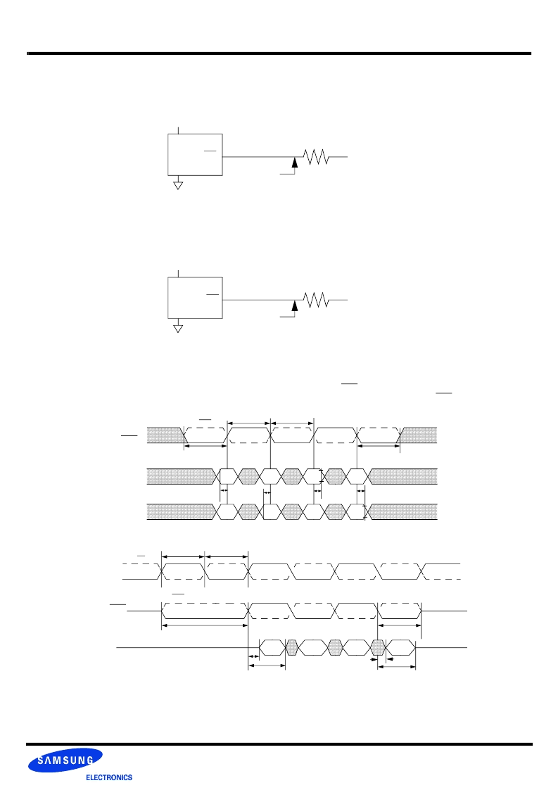
2. gDDR2 SDRAM AC timing reference load
Following figure represents the timing reference load used in defining the relevant timing parameters of the part. It is not intended to be either a precise
representation of the typical system environment or a depiction of the actual load presented by a production tester. System designers will use IBIS or
other simulation tools to correlate the timing reference load to a system environment. Manufacturers will correlate to their production test conditions (gen-
erally a coaxial transmission line terminated at the tester electronics).
VDDQ
The output timing reference voltage level for single ended signals is the crosspoint with VTT. The output timing reference voltage level for differential sig-
nals is the crosspoint of the true (e.g. DQS) and the complement (e.g. DQS) signal.
3. gDDR2 SDRAM output slew rate test load
Output slew rate is characterized under the test conditions as shown in the following figure.
VDDQ
4. Differential data strobe
gDDR2 SDRAM pin timings are specified for either single ended mode or differential mode depending on the setting of the EMRS “Enable DQS” mode
bit; timing advantages of differential mode are realized in system design. The method by which the gDDR2 SDRAM pin timings are measured is mode
dependent. In single ended mode, timing relationships are measured relative to the rising or falling edges of DQS crossing at VREF. In differential mode,
these timing relationships are measured relative to the crosspoint of DQS and its complement, DQS. This distinction in timing methods is guaranteed by
design and characterization. Note that when differential data strobe mode is disabled via the EMRS, the complementary pin, DQS, must be tied externally
to VSS through a 20 ohm
to 10 K ohm
resisor to insure proper operation.
DUT
DQ
DQS
DQS
Output
V
TT
= V
DDQ
/2
25
Timing
reference
point
<AC Timing Reference Load>
DUT
DQ
DQS, DQS
Output
V
TT
= V
DDQ
/2
25
Test point
<Slew Rate Test Load>
t
DS
t
DS
t
DH
t
WPRE
t
WPST
t
DQSH
t
DQSL
DQS
DQS
D
DMin
DQS/
DQS
DQ
DM
t
DH
<Data input (write) timing>
DMin
DMin
DMin
D
D
D
V
IL
(ac)
V
IH
(ac)
V
(ac)
V
IH
(ac)
V
IL
(dc)
V
IH
(dc)
V
IL
(dc)
V
IH
(dc)
t
CH
t
CL
CK
CK
CK/CK
DQS/DQS
DQ
DQS
DQS
t
RPST
Q
t
RPRE
t
DQSQmax
t
QH
t
QH
t
DQSQmax
<Data output (read) timing>
Q
Q
Q
相關(guān)PDF資料 |
PDF描述 |
|---|---|
| K4N51163QC-ZC33 | 512Mbit gDDR2 SDRAM |
| K4N51163QC-ZC36 | 512Mbit gDDR2 SDRAM |
| K4R271669B-N(M)CG6 | 256K x 16/18 bit x 32s banks Direct RDRAMTM |
| K4R271669B-N(M)CK7 | 256K x 16/18 bit x 32s banks Direct RDRAMTM |
| K4R271669B-Nb(M)CcK8 | 256K x 16/18 bit x 32s banks Direct RDRAMTM |
相關(guān)代理商/技術(shù)參數(shù) |
參數(shù)描述 |
|---|---|
| K4N51163QC-ZC33 | 制造商:SAMSUNG 制造商全稱:Samsung semiconductor 功能描述:512Mbit gDDR2 SDRAM |
| K4N51163QC-ZC36 | 制造商:SAMSUNG 制造商全稱:Samsung semiconductor 功能描述:512Mbit gDDR2 SDRAM |
| K4N51163QG | 制造商:SAMSUNG 制造商全稱:Samsung semiconductor 功能描述:Graphic Memory |
| K4N51163QZ | 制造商:SAMSUNG 制造商全稱:Samsung semiconductor 功能描述:Graphic Memory |
| K4N56163QF | 制造商:SAMSUNG 制造商全稱:Samsung semiconductor 功能描述:256Mbit gDDR2 SDRAM |
發(fā)布緊急采購,3分鐘左右您將得到回復(fù)。