- 您現(xiàn)在的位置:買賣IC網(wǎng) > PDF目錄374277 > K4N51163QC-ZC2A (SAMSUNG SEMICONDUCTOR CO. LTD.) 512Mbit gDDR2 SDRAM PDF資料下載
參數(shù)資料
| 型號(hào): | K4N51163QC-ZC2A |
| 廠商: | SAMSUNG SEMICONDUCTOR CO. LTD. |
| 英文描述: | 512Mbit gDDR2 SDRAM |
| 中文描述: | 512MB的GDDR2 SDRAM的 |
| 文件頁數(shù): | 22/64頁 |
| 文件大?。?/td> | 1420K |
| 代理商: | K4N51163QC-ZC2A |
第1頁第2頁第3頁第4頁第5頁第6頁第7頁第8頁第9頁第10頁第11頁第12頁第13頁第14頁第15頁第16頁第17頁第18頁第19頁第20頁第21頁當(dāng)前第22頁第23頁第24頁第25頁第26頁第27頁第28頁第29頁第30頁第31頁第32頁第33頁第34頁第35頁第36頁第37頁第38頁第39頁第40頁第41頁第42頁第43頁第44頁第45頁第46頁第47頁第48頁第49頁第50頁第51頁第52頁第53頁第54頁第55頁第56頁第57頁第58頁第59頁第60頁第61頁第62頁第63頁第64頁
- 22 -
Rev 1.5 Oct. 2005
512M gDDR2 SDRAM
K4N51163QC-ZC
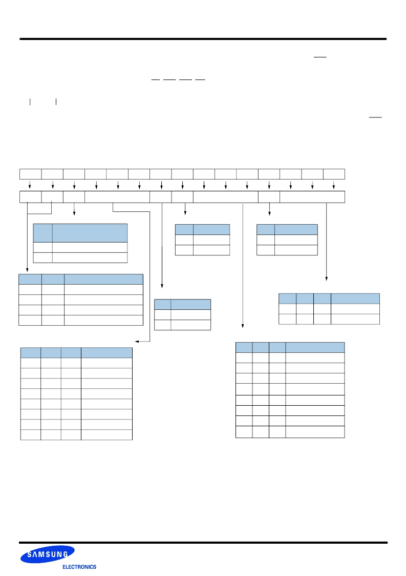
The mode register stores the data for controlling the various operating modes of gDDR2 SDRAM. It controls CAS latency, burst length,
burst sequence, test mode, DLL reset, tWR and various vendor specific options to make gDDR2 SDRAM useful for various applications.
The default value of the mode register is not defined, therefore the mode register must be written after power-up for proper operation.
The mode register is written by asserting low on CS, RAS, CAS, WE, BA0 and BA1, while controlling the state of address pins A0 ~
A15. The gDDR2 SDRAM should be in all bank precharge with CKE already high prior to writing into the mode register. The mode reg-
ister set command cycle time (tMRD) is required to complete the write operation to the mode register. The mode register contents can
be changed using the same command and clock cycle requirements during normal operation as long as all banks are in the precharge
state. The mode register is divided into various fields depending on functionality. Burst length is defined by A0 ~ A2 with options of 4 and
8 bit burst lengths. The burst length decodes are compatible with gDDR SDRAM. Burst address sequence type is defined by A3, CAS
latency is defined by A4 ~ A6. The gDDR2 doesn’t support half clock latency mode. A7 is used for test mode. A8 is used for DLL reset.
A7 must be set to low for normal MRS operation. Write recovery time tWR is defined by A9 ~ A11. Refer to the table for specific codes.
*1 : WR(write recovery for autoprecharge) min is determined by tCK max and WR max is determined by tCK min. WR in clock cycles
is calculated by dividing tWR (in ns) by tCK (in ns) and rounding up a non-integer value to the next integer
(WR[cycles] = tWR(ns)/tCK(ns)). The mode register must be programmed to this value. This is also used with tRP to determine tDAL.
CAS Latency
A6
A5
A4
Latency
0
0
0
Reserved
0
0
1
Reserved
0
1
0
Reserved
0
1
1
3
1
0
0
4
1
0
1
5
1
1
0
6
1
1
1
Reserved
Burst Length
A2
A1
A0
Burst Length
0
1
0
4
0
1
1
8
Burst Type
A3
Type
0
Sequential
1
Interleave
BA
1
BA
0
A
12
A
11
A
10
A
9
A
8
A
7
A
6
A
5
A
4
A
3
A
2
A
1
A
0
BA1
BA0
MRS Mode
0
0
MRS
0
1
EMRS (1)
1
0
EMRS (2) : Reserved
1
1
EMRS (3) : Reserved
DLL
A8
DLL Reset
0
No
1
Yes
Test Mode
A7
mode
0
Normal
1
Test
0
0
PD
tWR
*1
DLL
TM
CAS Latency
BT
Burst Length
A12
Active Power
Down exit time
0
Fast exit (use tXARD)
1
Slow exit (use tXARDS)
Write Recovery for Auto Precharge
A11
A10
A9
MRS Select
0
0
0
Reserved
0
0
1
Reserved
0
1
0
3
0
1
1
4
1
0
0
5
1
0
1
Reserved
1
1
0
Reserved
1
1
1
Reserved
gDDR2 SDRAM Mode Register Set (MRS)
Address Bus
Mode Register
相關(guān)PDF資料 |
PDF描述 |
|---|---|
| K4N51163QC-ZC33 | 512Mbit gDDR2 SDRAM |
| K4N51163QC-ZC36 | 512Mbit gDDR2 SDRAM |
| K4R271669B-N(M)CG6 | 256K x 16/18 bit x 32s banks Direct RDRAMTM |
| K4R271669B-N(M)CK7 | 256K x 16/18 bit x 32s banks Direct RDRAMTM |
| K4R271669B-Nb(M)CcK8 | 256K x 16/18 bit x 32s banks Direct RDRAMTM |
相關(guān)代理商/技術(shù)參數(shù) |
參數(shù)描述 |
|---|---|
| K4N51163QC-ZC33 | 制造商:SAMSUNG 制造商全稱:Samsung semiconductor 功能描述:512Mbit gDDR2 SDRAM |
| K4N51163QC-ZC36 | 制造商:SAMSUNG 制造商全稱:Samsung semiconductor 功能描述:512Mbit gDDR2 SDRAM |
| K4N51163QG | 制造商:SAMSUNG 制造商全稱:Samsung semiconductor 功能描述:Graphic Memory |
| K4N51163QZ | 制造商:SAMSUNG 制造商全稱:Samsung semiconductor 功能描述:Graphic Memory |
| K4N56163QF | 制造商:SAMSUNG 制造商全稱:Samsung semiconductor 功能描述:256Mbit gDDR2 SDRAM |
發(fā)布緊急采購(gòu),3分鐘左右您將得到回復(fù)。