- 您現(xiàn)在的位置:買賣IC網(wǎng) > PDF目錄374277 > K4N51163QC-ZC2A (SAMSUNG SEMICONDUCTOR CO. LTD.) 512Mbit gDDR2 SDRAM PDF資料下載
參數(shù)資料
| 型號: | K4N51163QC-ZC2A |
| 廠商: | SAMSUNG SEMICONDUCTOR CO. LTD. |
| 英文描述: | 512Mbit gDDR2 SDRAM |
| 中文描述: | 512MB的GDDR2 SDRAM的 |
| 文件頁數(shù): | 40/64頁 |
| 文件大小: | 1420K |
| 代理商: | K4N51163QC-ZC2A |
第1頁第2頁第3頁第4頁第5頁第6頁第7頁第8頁第9頁第10頁第11頁第12頁第13頁第14頁第15頁第16頁第17頁第18頁第19頁第20頁第21頁第22頁第23頁第24頁第25頁第26頁第27頁第28頁第29頁第30頁第31頁第32頁第33頁第34頁第35頁第36頁第37頁第38頁第39頁當(dāng)前第40頁第41頁第42頁第43頁第44頁第45頁第46頁第47頁第48頁第49頁第50頁第51頁第52頁第53頁第54頁第55頁第56頁第57頁第58頁第59頁第60頁第61頁第62頁第63頁第64頁
- 40 -
Rev 1.5 Oct. 2005
512M gDDR2 SDRAM
K4N51163QC-ZC
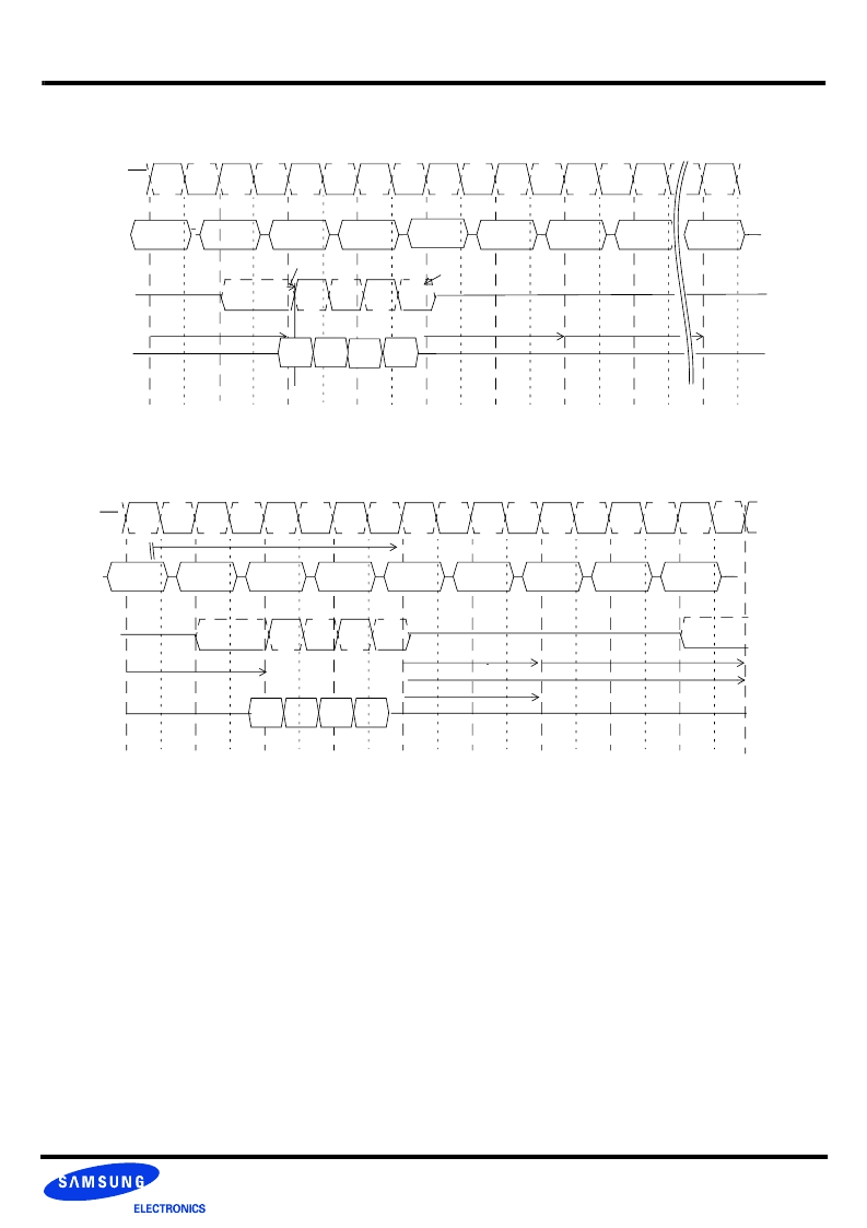
Burst Write Operation: RL = 3, WL = 2, tWR = 2 (AL=0, CL=3), BL = 4
CMD
NOP
NOP
NOP
NOP
Precharge
NOP
DQs
NOP
CK/CK
T0
T2
T1
T3
T4
T5
T6
T7
Tn
WRITE A
CAS
WL = RL - 1 = 2
DQS
< = t
DQSS
> = WR
DIN A
0
DIN A
1
DIN A
2
DIN A
3
Bank A
Activate
Completion of
the Burst Write
> = tRP
Burst Write followed by Burst Read: RL = 5 (AL=2, CL=3), WL = 4, tWTR = 2, BL = 4
CMD
NOP
NOP
NOP
NOP
DQ
CK/CK
T0
T2
T1
T3
T4
T5
T6
T7
T8
DOUT A
0
DOUT A
1
DOUT A
2
DOUT A
3
NOP
DQS
WL = RL - 1 = 4
Post CAS
READ A
NOP
RL =5
AL = 2
CL = 3
NOP
NOP
Write to Read = CL - 1 + BL/2 + tWTR
> = tWTR
T9
The minimum number of clock from the burst write command to the burst read command is [CL - 1 + BL/2 + tWTR]. This tWTR is not a
write recovery time (tWR) but the time required to transfer the 4bit write data from the input buffer into sense amplifiers in the array.
tWTR is defined in AC spec table of this data sheet.
相關(guān)PDF資料 |
PDF描述 |
|---|---|
| K4N51163QC-ZC33 | 512Mbit gDDR2 SDRAM |
| K4N51163QC-ZC36 | 512Mbit gDDR2 SDRAM |
| K4R271669B-N(M)CG6 | 256K x 16/18 bit x 32s banks Direct RDRAMTM |
| K4R271669B-N(M)CK7 | 256K x 16/18 bit x 32s banks Direct RDRAMTM |
| K4R271669B-Nb(M)CcK8 | 256K x 16/18 bit x 32s banks Direct RDRAMTM |
相關(guān)代理商/技術(shù)參數(shù) |
參數(shù)描述 |
|---|---|
| K4N51163QC-ZC33 | 制造商:SAMSUNG 制造商全稱:Samsung semiconductor 功能描述:512Mbit gDDR2 SDRAM |
| K4N51163QC-ZC36 | 制造商:SAMSUNG 制造商全稱:Samsung semiconductor 功能描述:512Mbit gDDR2 SDRAM |
| K4N51163QG | 制造商:SAMSUNG 制造商全稱:Samsung semiconductor 功能描述:Graphic Memory |
| K4N51163QZ | 制造商:SAMSUNG 制造商全稱:Samsung semiconductor 功能描述:Graphic Memory |
| K4N56163QF | 制造商:SAMSUNG 制造商全稱:Samsung semiconductor 功能描述:256Mbit gDDR2 SDRAM |
發(fā)布緊急采購,3分鐘左右您將得到回復(fù)。